Method for manufacturing a liquid crystal display
A technology of liquid crystal display and manufacturing method, applied in the input/output process of data processing, optics, instruments, etc., can solve problems such as misoperation of PCB board wiring, signal interference, complexity, etc., and achieve reduction of misoperation and low wiring density , the effect of increased line spacing
- Summary
- Abstract
- Description
- Claims
- Application Information
AI Technical Summary
Problems solved by technology
Method used
Image

Examples
Embodiment 1
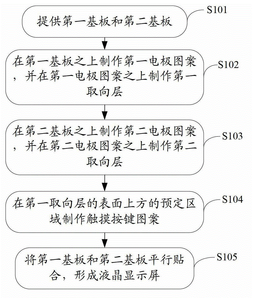
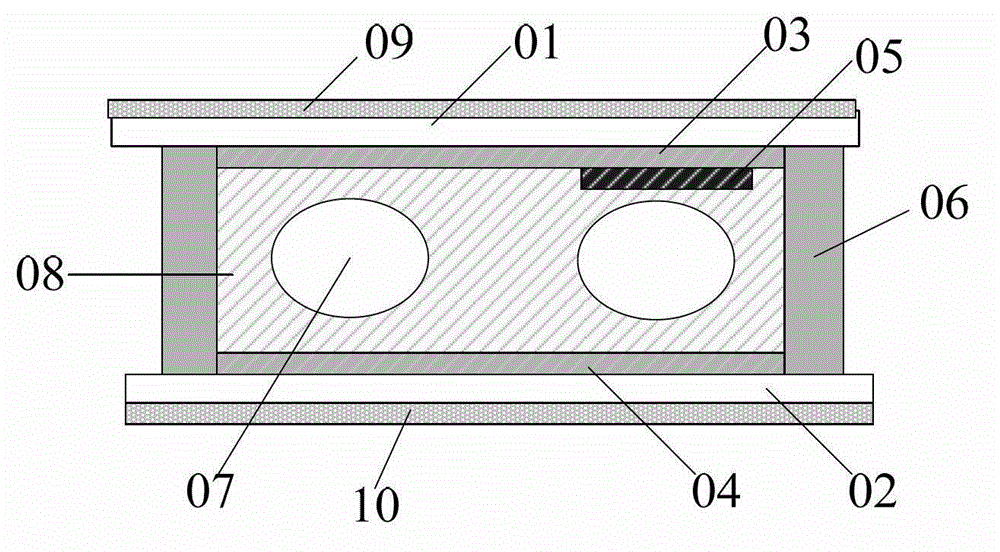
[0070] FIG. 1( a ) is a flow chart of a manufacturing method of a liquid crystal display in Embodiment 1 of the present invention, and FIG. 1( b ) is a schematic structural diagram of a liquid crystal display in Embodiment 1 of the present invention.
[0071] The manufacturing method of the liquid crystal display in the embodiment 1 comprises the following steps:
[0072] S101. Providing a first substrate and a second substrate:
[0073] A first substrate and a second substrate for making a liquid crystal display are provided. The first substrate 01 and the second substrate 02 are shown in FIG. 1( b ). The two substrates may be the upper substrate and the lower substrate of the liquid crystal display screen respectively. The substrate is generally a transparent substrate, which can be made of glass material, or polyethylene terephthalate (PET), polycarbonate (PC), polymethyl methacrylate (PMMA), polyethylene naphthalate Ethylene glycol ester (PEN), polyethersulfone (PES), c...
Embodiment 2
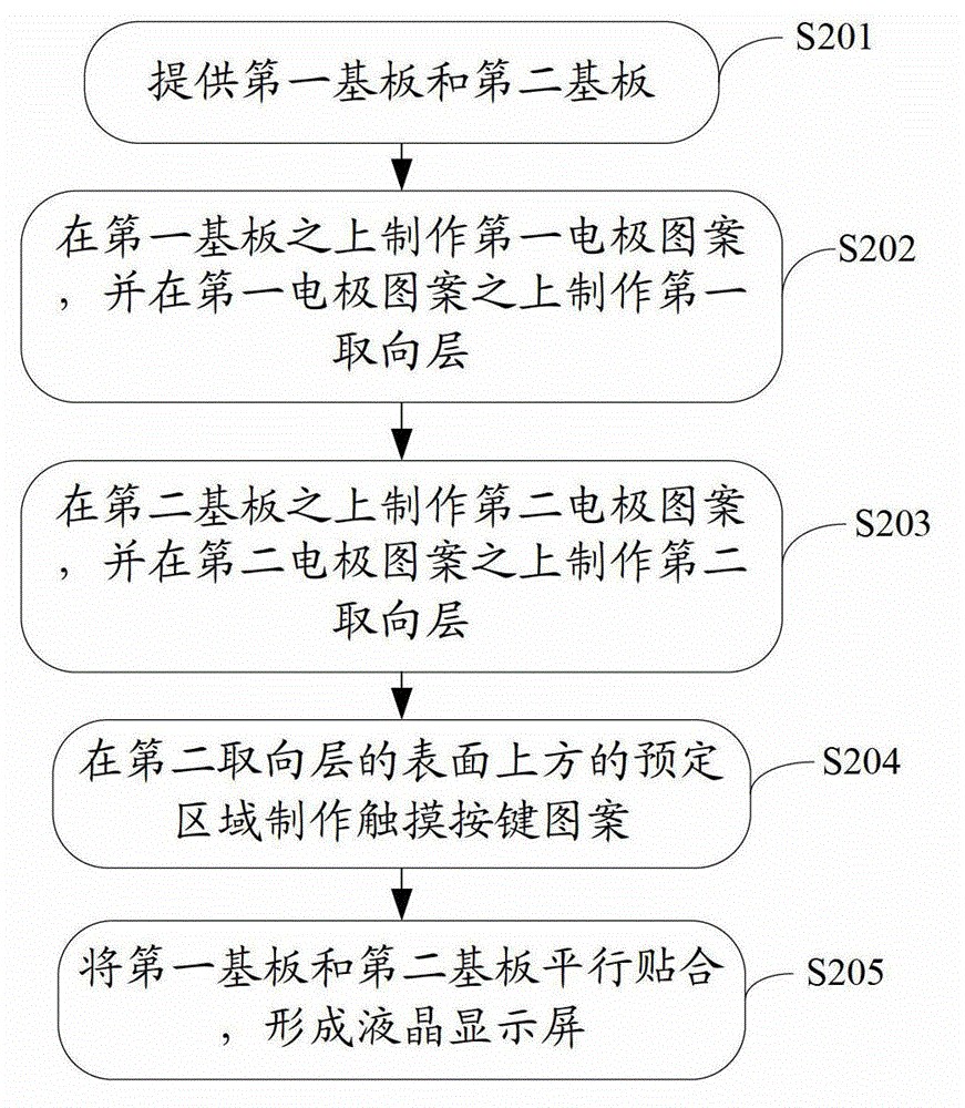
[0093] FIG. 2( a ) is a flowchart of a manufacturing method of a liquid crystal display according to Embodiment 2 of the present invention, and FIG. 2( b ) is a schematic structural diagram of a liquid crystal display according to Embodiment 2 of the present invention.
[0094] The liquid crystal display and its manufacturing method of the example of the second embodiment have many similarities with the liquid crystal display of the example of the first embodiment and its manufacturing method. For the sake of brevity, this embodiment only describes the differences in detail. The same Please refer to Embodiment 1 for details.
[0095] Steps S201-S203 in the method for manufacturing a liquid crystal display in Embodiment 2 are the same as steps S101-S103 in the method for manufacturing a liquid crystal display in Embodiment 1. For the sake of brevity, they will not be described in detail here. For more information, please refer to Refer to the description of Embodiment 1.
[00...
Embodiment 3
[0105] The liquid crystal display and its manufacturing method of the third embodiment have many similarities with the liquid crystal display and its manufacturing method of the first embodiment. For the sake of brevity, this embodiment only describes the differences in detail. The same Please refer to Embodiment 1 for details.
[0106] FIG. 3( a ) is a flowchart of a manufacturing method of a liquid crystal display according to Embodiment 3 of the present invention, and FIG. 3( b ) is a schematic structural diagram of a liquid crystal display according to Embodiment 3 of the present invention. The manufacturing method of the liquid crystal display of the present embodiment comprises the following steps:
[0107] S301. Providing a first substrate and a second substrate:
[0108] Step S301 is the same as step S101 in Embodiment 1. For the sake of brevity, no detailed description is given here. For specific description, please refer to Embodiment 1.
[0109] S302. Fabricate a ...
PUM
 Abstract
Description
Claims
Application Information
 - Generate Ideas
- Intellectual Property
- Life Sciences
- Materials
- Tech Scout
- Unparalleled Data Quality
- Higher Quality Content
- 60% Fewer Hallucinations
Browse by: Latest US Patents, China's latest patents, Technical Efficacy Thesaurus, Application Domain, Technology Topic, Popular Technical Reports.
© 2025 PatSnap. All rights reserved.Legal|Privacy policy|Modern Slavery Act Transparency Statement|Sitemap|About US| Contact US: help@patsnap.com