Etching method of contact hole

A contact hole, dry etching technology, applied in electrical components, semiconductor/solid-state device manufacturing, circuits, etc., can solve problems such as poor contact hole morphology

Active Publication Date: 2013-04-17
深圳深爱半导体股份有限公司
View PDF9 Cites 14 Cited by
  • Summary
  • Abstract
  • Description
  • Claims
  • Application Information

AI Technical Summary

Problems solved by technology

[0004] Based on this, it is necessary to solve the problem of poor contact hole morphology etched by traditional contact hole etching methods, and provide a contact hole etching method that can obtain better contact hole morphology and thereby obtain good device performance. Eclipse method

Method used


Image

  • Etching method of contact hole
  • Etching method of contact hole
  • Etching method of contact hole

Examples


Embodiment Construction

[0017] In order to make the objects, features and advantages of the present invention more comprehensible, specific implementations of the present invention will be described in detail below in conjunction with the accompanying drawings.

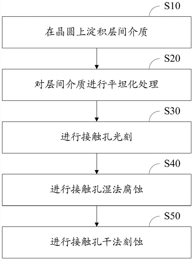
[0018] image 3 It is a flowchart of the etching method of a contact hole in an embodiment, comprising the following steps:

[0019] S10, depositing an interlayer dielectric on the wafer.

[0020] The deposited interlayer dielectric covers the polysilicon gate on the substrate. The interlayer dielectric can be phosphosilicate glass (PSG) or borophosphosilicate glass (BPSG).

[0021] S20, planarizing the interlayer dielectric.

[0022] The interlayer dielectric can be planarized with chemical mechanical polishing (CMP).

[0023] S30 , performing contact hole photolithography.

[0024] A photoresist is applied and the contact hole area is defined by exposure and development.

[0025] S40, performing contact hole wet etching.

[0026] Et...


PUM


Abstract

The invention relates to an etching method of a contact hole. The method comprises the following steps of: depositing an interlayer dielectric on a wafer; flattening the interlayer dielectric; etching the contact hole; performing contact hole wet etching, and etching 30%-70% thickness of the interlayer dielectric; and performing contact hole dry etching. Through two steps of etching technologies, the wet etching uses the isotropic characteristics of the etching, so that the interlayer dielectric is in bowl-like appearance at the steps of the contact hole; and the dry etching uses the anisotropic of the dry etching, so that the appearance of the steps is approximate to a right angle. Through the combination of the wet etching and the drying etching, the steps at the contact hole are smooth without large closed angle; a metal layer can be avoided from generating cavities at the closed angle at the edge of the contact hole; the interlayer dielectric can be ensured to have enough thickness at the steps of polysilicon gates; and enough BVDSS (drain-source breakdown voltage) can be guaranteed.

Description

technical field [0001] The invention relates to a manufacturing process of a semiconductor device, in particular to an etching method for a contact hole. Background technique [0002] In the semiconductor manufacturing process, there are usually two types of contact holes: one is the contact hole on the active region, and the other is the contact hole on the polysilicon gate. [0003] figure 1 It is a photo under a microscope after the contact hole is etched by a traditional dry method. It can be seen that after the metal is deposited, the metal will generate holes at the sharp corners of the phosphosilicate glass layer. And if wet etching is used, as figure 2 As shown, the slope of the phosphosilicate glass layer 120 is closer to the inner polysilicon 110 after etching, and the drain-source breakdown voltage (BVDSS) is smaller, which makes the device easily broken down. Contents of the invention [0004] Based on this, it is necessary to solve the problem of poor cont...

Claims


Application Information

Patent Timeline
Patent Type & Authority Applications(China)
IPC IPC(8): H01L21/768H01L21/311
Inventor 王民涛李杰汪德文魏国栋刘玮杨坤进
Owner 深圳深爱半导体股份有限公司
Why Eureka
Try Eureka