Embedded non-volatile memory provided with P+ single polycrystalline architecture of selector transistor and free of light doped regions and preparation method of embedded non-volatile memory

A non-volatile, transistor-based technology, applied in semiconductor/solid-state device manufacturing, electric solid-state devices, semiconductor devices, etc., can solve the problem of large ratio of control circuit area, achieve compact structure, reduce processing costs, and improve adaptability

Active Publication Date: 2013-04-03
浙江锋华创芯微电子有限公司
View PDF5 Cites 2 Cited by
  • Summary
  • Abstract
  • Description
  • Claims
  • Application Information

AI Technical Summary

Problems solved by technology

In this case, the proportion of the area occupied by the peripheral control circuit will be very large.

Method used


Image

  • Embedded non-volatile memory provided with P+ single polycrystalline architecture of selector transistor and free of light doped regions and preparation method of embedded non-volatile memory
  • Embedded non-volatile memory provided with P+ single polycrystalline architecture of selector transistor and free of light doped regions and preparation method of embedded non-volatile memory
  • Embedded non-volatile memory provided with P+ single polycrystalline architecture of selector transistor and free of light doped regions and preparation method of embedded non-volatile memory

Examples


Embodiment 1

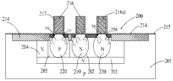
[0068] like figure 1 and Figure 13 Shown: In order to make the non-volatile memory compatible with the CMOS logic process and enable the non-volatile memory to store for a longer period of time, the non-volatile memory includes a P conductivity type substrate 201, a P conductivity type substrate 201 The material is silicon. The upper part of the P conductivity type substrate 201 is provided with at least one memory cell 200, and the memory cell 200 includes a PMOS transistor 210 without a lightly doped region, a control capacitor 220 and a PMOS selector transistor 230, and the P conductivity type substrate 201 A gate dielectric layer 215 is deposited and covered on the surface, and the gate dielectric layer 215 covers the surface corresponding to the formation of the memory cell 200, and the area between the PMOS transistor 210 and the control capacitor 220 without the lightly doped area passes through the area in the P conductivity type substrate 201 The dielectric region ...

Embodiment 2

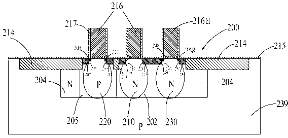
[0094] like figure 2 and Figure 23 As shown: in this embodiment, the semiconductor substrate is an N-conductive type substrate 239. When the N-conductive type substrate 239 is used, there is no need to form the second N-type region 203 and the second P-type region 205 in the N-conductive type substrate 239 to directly contact with the second P-type region 205. The N-type conductive type substrate 239 is in contact with, and at the same time, the first N-type region 202 and the third N-type region 204 are also in direct contact with the N-type conductive type substrate 239 . After adopting the substrate 239 of N conductivity type, the rest of the structure is the same as that of Embodiment 1.

[0095] like Figure 14~Figure 23 Shown: the non-volatile memory of the above structure can be realized through the following process steps, specifically:

[0096] a. An N conductive type substrate 239 is provided, and the N conductive type substrate 239 includes a first main surface...


PUM


Abstract

The invention relates to an embedded non-volatile memory provided with a P+ single polycrystalline architecture of a selector transistor, free of light doped regions and compatible with the CMOS (complementary metal oxide semiconductor) process and a preparation method of the embedded non-volatile memory. The embedded non-volatile memory comprises a semiconductor substrate and a memory cell, the memory cell comprises a PMOS (P-channel metal oxide semiconductor) transistor without the light doped regions, a control capacitor and the PMOS selector transistor, a gate dielectric layer is deposited on the surface of the semiconductor substrate, a floating gate electrode is arranged on the gate dielectric layer and covers and penetrates through the PMOS transistor without the light doped regions and the corresponding gate dielectric layer above the control capacitor, side protecting layers are deposited on two sides of the floating gate electrode, the PMOS transistor without the light doped regions comprises a first N-type region, a P-type source electrode region and a P-type drain electrode region, and the control capacitor comprises a second P-type region, a first P-type doped region and a second P-type doped region. The embedded non-volatile memory is compact in structure and compatible with the CMOS process, chip cost is reduced, and storage safety and reliability are improved.

Description

technical field [0001] The invention relates to a non-volatile memory and a preparation method thereof, in particular to an embedded non-volatile memory with a P+ single polycrystalline structure having a selector transistor, no lightly doped region and compatible with a CMOS process The invention and a preparation method thereof belong to the technical field of integrated circuits. Background technique [0002] For system-on-chip (SoC) applications, it is the integration of many functional blocks into an integrated circuit. The most common SoCs include a microprocessor or microcontroller, static random access memory (SRAM) modules, non-volatile memory, and logic blocks for various special functions. However, conventional non-volatile memory processes, which typically use stacked-gate or split-gate memory cells, are not compatible with conventional logic processes. [0003] Non-volatile memory (NVM) technology is different from traditional logic technology. The combinatio...

Claims


Application Information

Patent Timeline
Patent Type & Authority Applications(China)
IPC IPC(8): H01L27/115H01L21/8247H10B41/35H10B69/00H10B41/41
Inventor 不公告发明人
Owner 浙江锋华创芯微电子有限公司
Why Eureka
Try Eureka