Amorphous carbon processing method and etching method by adopting amorphous carbon as hard mask

A technology of amorphous carbon and processing methods, which is applied in the fields of electrical components, semiconductor/solid-state device manufacturing, circuits, etc., can solve the problems of high process requirements for hard mask layer and limited range of boron doping dose, etc., and achieve precise etching process, Unlimited effect of boron doping dose range

Active Publication Date: 2013-04-03
SEMICON MFG INT (SHANGHAI) CORP
View PDF4 Cites 9 Cited by
  • Summary
  • Abstract
  • Description
  • Claims
  • Application Information

AI Technical Summary

Problems solved by technology

[0013] The problem solved by the present invention is to propose a new processing method of amorphous carbon as a hard mask and an etching method using amorphous carbon as a hard mask to overcome the existing process of using amorphous carbon as a hard mask. When etching, the range of boron doping dose is limited and the process requirements are high when removing the hard mask layer

Method used


Image

  • Amorphous carbon processing method and etching method by adopting amorphous carbon as hard mask
  • Amorphous carbon processing method and etching method by adopting amorphous carbon as hard mask
  • Amorphous carbon processing method and etching method by adopting amorphous carbon as hard mask

Examples


Embodiment Construction

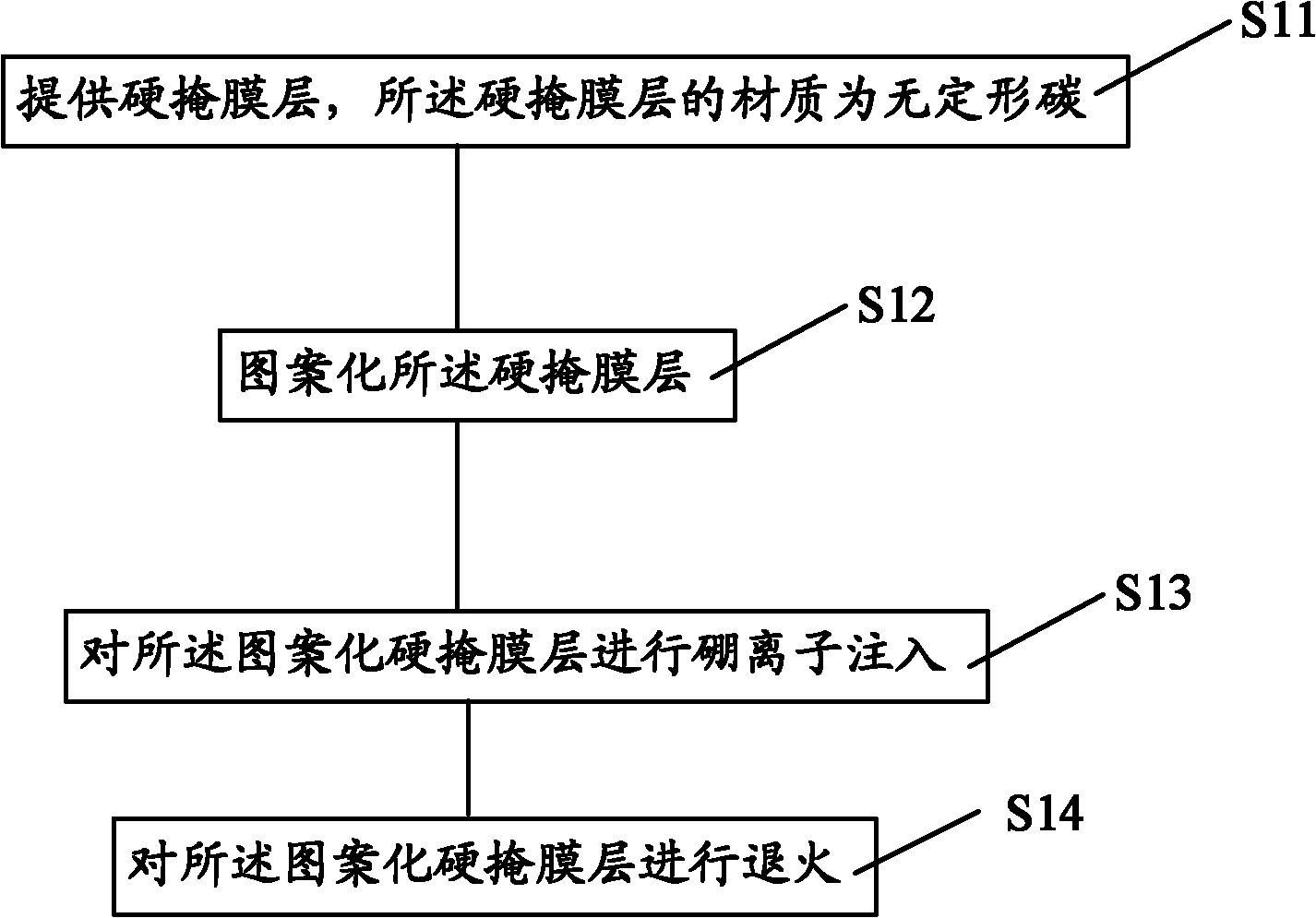
[0055]In the present invention, the pattern on the mask plate is first aligned with the pattern of the amorphous carbon detection alignment mark and the substrate, and then the hard mask layer is patterned; The improvement of the light transmittance becomes worse, which affects the alignment accuracy; after that, boron ion implantation is performed on the patterned hard mask layer to form a new patterned hard mask layer, and the new patterned hard mask layer As a mask, the layer to be etched is etched, so that the entire etching process is precise and the boron dosage range is not limited.

[0056] In addition, the boron ion implantation is carried out after the hard mask layer has been patterned, in other words, only boron ions are contained on the surface of the amorphous carbon. Since the hard mask layer is mainly used for the surface layer during the etching process, Therefore, it acts as a hard mask, and when the hard mask is removed later, the surface area only needs to ...


PUM


Abstract

The invention provides a method of processing the amorphous carbon which serves as a hard mask. The method comprises the steps of: providing a hard mask layer which is made of amorphous carbon; patterning the hard mask layer; and conducting boron ion injection on the patterned hard mask layer. The invention further provides an etching method by adopting amorphous carbon as the hard mask, and comprises the steps of: providing a semiconductor substrate, forming an aligned mark and substrate patterns on the semiconductor substrate, wherein a layer to be etched is arranged at the uppermost layer; depositing the hard mask layer on the layer to be etched, wherein the hard mask layer is made of the amorphous carbon; detecting the aligned mark through the amorphous carbon so as to align patterns on a mask edition to the substrate patterns; patterning the hard mask layer; conducting boron ion injection on the patterned hard mask layer to form a new patterned hard mask layer; and etching the layer to be etched by taking the new patterned hard mask layer as a mask. According to the technical scheme, the problems that boron doping amount is limited when the to-be-etched layer is etched and the process requirement is high when the hard mask layer is removed can be solved.

Description

technical field [0001] The invention relates to the field of semiconductor manufacturing, in particular to a treatment method of amorphous carbon used as a hard mask and an etching method using amorphous carbon as a hard mask. Background technique [0002] In today's semiconductor manufacturing process, due to the thinner and thinner photoresist used in advanced photolithography technology, and the need to maintain etch selectivity at the same time, the use of hard masks is becoming more and more widespread. [0003] Amorphous carbon as a hard mask has some advantages that other materials do not have: first, amorphous carbon has better light transmission, which is more conducive to layer alignment (overlap) in lithography; second, amorphous carbon hardness Larger, compared with other materials, it has a high etching selectivity ratio; third, amorphous carbon is a very easy to remove material. [0004] In order to further improve the etching selectivity ratio of amorphous ca...

Claims


Application Information

Patent Timeline
IPC IPC(8): H01L21/3105H01L21/314H01L21/311H01L21/027
Inventor 邓浩张彬
Owner SEMICON MFG INT (SHANGHAI) CORP
Why Eureka
Try Eureka