
Delay circuit

A technology of delay circuit and external circuit, applied in electrical components, electronic switches, pulse technology, etc., can solve the problem of cost delay circuit prolonging time and other problems, and achieve the requirements of reducing resistance value, reducing capacitance requirements, and reducing cost. Effect

Inactive Publication Date: 2013-03-27
JIANGSU GELITE ELECTRONICS
View PDF4 Cites 4 Cited by
  • Summary
  • Abstract
  • Description
  • Claims
  • Application Information

AI Technical Summary

Problems solved by technology

[0003] The problem to be solved by the present invention is to provide a delay circuit, which can solve the problem that the cost of manufacturing chips in the prior art is greatly affected by the extension time of the delay circuit

Method used


Image

  • Delay circuit
  • Delay circuit

Examples


Embodiment Construction

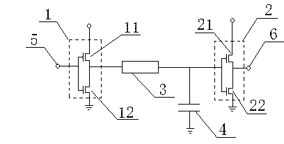
[0010] Such as figure 1 The delay circuit shown in the prior art includes a first CMOS inverter 1 composed of a first PMOS transistor 11 and a first NMOS transistor 12, and a first CMOS inverter 1 composed of a second PMOS transistor 21 and a second NMOS transistor 22. Two CMOS inverters 2, the input terminal 5 of the first CMOS inverter 1 receives an input signal, the output terminal of the first CMOS inverter 1 is connected to one end of a resistor 3, and the other ends of the resistor 3 are respectively It is connected with the capacitor 4 with one end grounded and the input end of the second CMOS inverter 2, and the output end 6 of the second CMOS inverter 2 is connected with the external circuit.

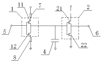
[0011] Such as figure 2 The delay circuit shown, with figure 1 The difference is that: the source of the first PMOS transistor 11 is provided with a resistor 7 to connect to the power supply, the source of the first NMOS transistor 12 is provided with a resistor 8 to ground,...


PUM


Abstract

The invention discloses a delay circuit and relates to the design field of integrated chips. The delay circuit comprises a first complementary metal oxide semiconductor (CMOS) inverter composed of a first p-channel metal oxide semiconductor (PMOS) pipe and a first n-channel metal oxide semiconductor (NMOS) pipe and a second CMOS inverter composed of a second PMOS pipe and a second NMOS pipe. The input end of the first CMOS inverter receives input signals, and the output end of the first CMOS inverter is respectively connected with a capacitor with one end connected with the ground and the input end of the second CMOS inverter. The output end of the second CMOS inverter is connected with an outer circuit, a source of the first PMOS pipe is provided with a resistor and connected with a power supply, and the source of the first NMOS pipe is provided with a resistor and connected with the ground. By arranging the resistors on the sources of the first PMOS pipe and the first NOMS pipe, the resistors are amplified through a metal oxide semiconductor (MOS) pipe, requirements of the delay circuit for resistance of the resistors are lowered, and simultaneously a requirement for capacitance of the capacitor is also reduced, and therefore the cost of the delay circuit is reduced.

Description

technical field [0001] The invention relates to the field of integrated circuit design, in particular to a delay circuit. Background technique [0002] In the design of integrated circuits, it is necessary to use a delay circuit to realize the timing control between various signals. The general delay circuit realizes the delay function through an RC circuit composed of a resistor and a capacitor, and the input signal passes through the first CMOS inverter. Input the RC circuit, and then output through the second COMS inverter to complete the delay function of the input signal and the output signal; in the integrated circuit process, the capacitance of the capacitor can only be within 10P, otherwise the area of ​​the capacitor will be relative to the area of ​​the chip Too large will affect the manufacturing cost of the chip; in the case of a capacitor of 10p, if the delay is 100ns, the resistance of the resistor needs to reach 10k ohms. For conventional poly resistors, the c...

Claims


Application Information

Patent Timeline
Patent Type & Authority Applications(China)
IPC IPC(8): H03K17/28
Inventor 谢卫国
Owner JIANGSU GELITE ELECTRONICS
Learn More