Noise suppression method, device and LTE digital microwave radio frequency remote coverage system
A noise suppression, digital microwave technology, applied in the field of communication, can solve the problem of raising the noise floor of the base station, and achieve the effect of increasing flexibility, improving uplink coverage and uplink throughput, and avoiding the noise floor being raised.
- Summary
- Abstract
- Description
- Claims
- Application Information
AI Technical Summary
Problems solved by technology
Method used
Image
Examples
Embodiment 1
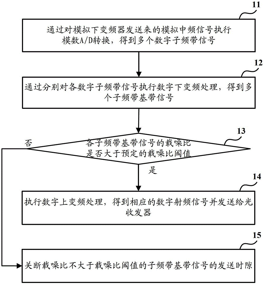
[0029] Such as figure 1 As shown, it is a main flowchart of a noise suppression method provided by Embodiment 1 of the present invention, which is applied to the remote microwave transmission system of the LTE digital microwave radio remote coverage system. The method includes the following steps:
[0030] Step 11, by performing analog-to-digital A / D conversion on the analog intermediate frequency signal sent by the analog down-converter, to obtain a plurality of digital sub-band signals;
[0031] Specifically, in this step 11, the uplink LTE radio frequency signal transmitted by the user terminal is received from the space through the coverage or receiving antenna, and the uplink radio frequency signal is obtained after filtering out unnecessary signals. Amplify, and after analog down-conversion processing by the analog down-converter, down-convert the uplink intermediate frequency signal to an analog intermediate frequency signal, and then perform A / D conversion sampling on ...
Embodiment 2
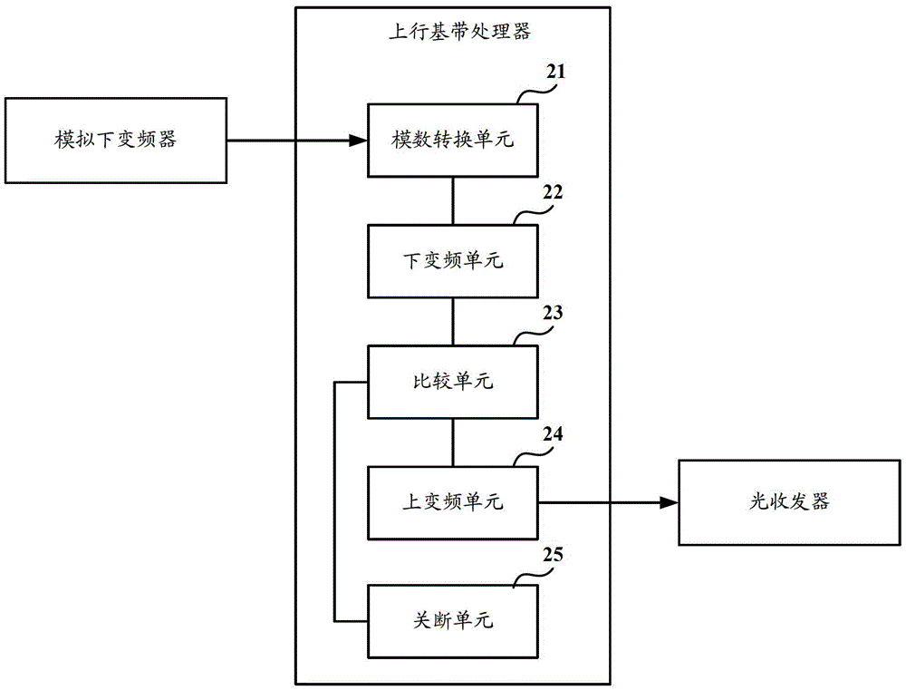
[0044] Correspondingly, Embodiment 2 of the present invention provides a noise suppression device. Embodiment 2 of the present invention is a device under the same concept as Embodiment 1 of the present invention, and is applied to the remote microwave of the LTE digital microwave radio remote coverage system. In the transmission system, such as figure 2 Shown is a schematic structural diagram of the noise suppression device, including:
[0045] The analog-to-digital conversion unit 21 is configured to obtain a plurality of digital sub-band signals by performing analog-to-digital A / D conversion on the analog intermediate frequency signal sent by the analog down-converter;
[0046] The down-conversion unit 22 is used to obtain a plurality of sub-band baseband signals by performing digital down-conversion processing on the digital sub-band signals obtained by the analog-to-digital conversion unit 21 respectively;
[0047] The comparison unit 23 is used to compare the carrier-t...
Embodiment 3
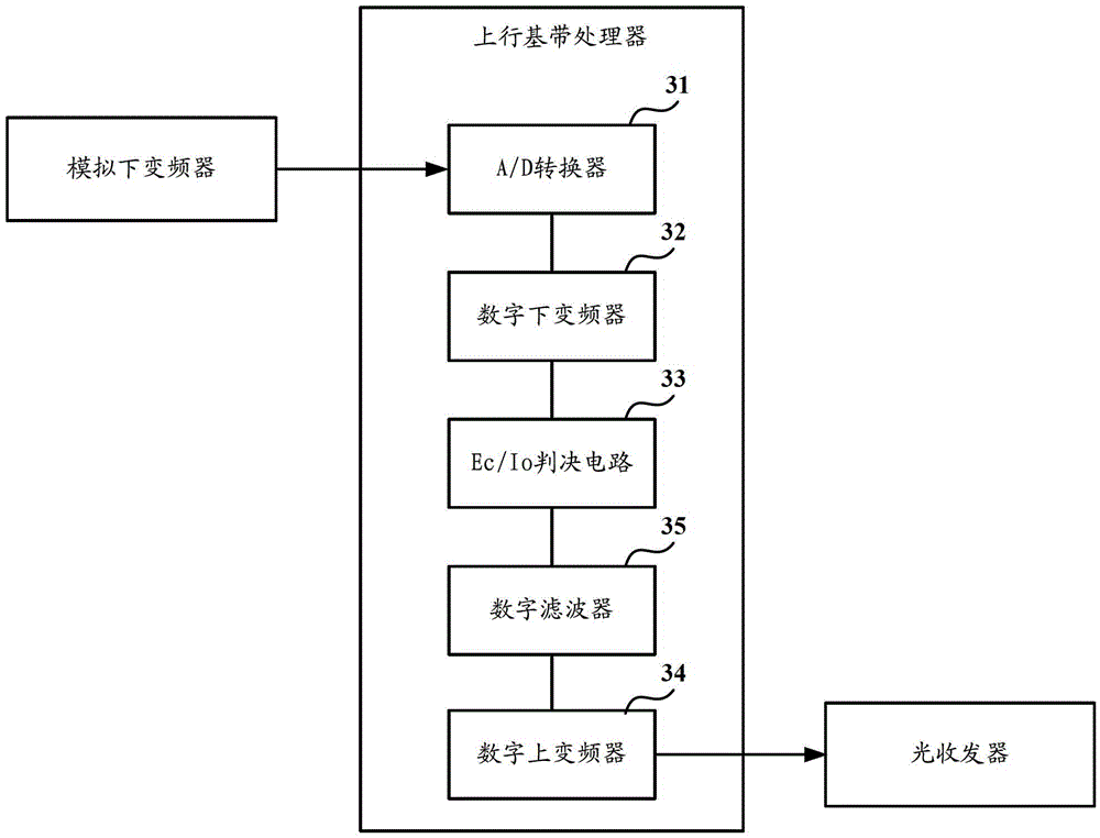
[0056] Such as image 3 As shown, it is a schematic diagram of the internal structure of an uplink baseband processor provided by Embodiment 3 of the present invention, which includes: an analog-to-digital A / D converter 31, a digital down-converter DDC32, and a carrier-to-noise ratio Ec / Io decision circuit 33 and digital upconverter DUC34, where,
[0057] The A / D converter 31 is connected with the digital down-converter DDC32, performs analog-to-digital A / D conversion on the analog intermediate frequency signal sent by the analog down-converter, and sends the obtained multiple digital sub-band signals to the digital down-converter DDC32 ;
[0058] Digital down-converter DDC32 is connected with Ec / Io decision circuit 33, after carrying out digital down-conversion processing to each digital sub-band signal respectively, a plurality of sub-band baseband signals obtained are used as the input signal of Ec / Io decision circuit 33;
[0059] The Ec / Io decision circuit 33 is connecte...
PUM
 Abstract
Description
Claims
Application Information
 - R&D
- Intellectual Property
- Life Sciences
- Materials
- Tech Scout
- Unparalleled Data Quality
- Higher Quality Content
- 60% Fewer Hallucinations
Browse by: Latest US Patents, China's latest patents, Technical Efficacy Thesaurus, Application Domain, Technology Topic, Popular Technical Reports.
© 2025 PatSnap. All rights reserved.Legal|Privacy policy|Modern Slavery Act Transparency Statement|Sitemap|About US| Contact US: help@patsnap.com


