
Patsnap Eureka
For R&D, Patsnap Eureka makes reading and utilizing patents & technical documents easy.
Patsnap Eureka AIR
Designed for self-driven R&D workflows. Generate viable solutions, solve complex R&D challenges, empower your innovation with AI.

Patsnap Eureka Materials
Designed for material experts only. Revolutionize your material R&D, from search, analyze, to developing new materials.

TechResearch
Generate reliable direction feasibility study reports for your R&D in just a few steps.

TechSeek
Discover and master advanced knowledge NOW. Basics, ideas, possibilities, all at once.

TechMind
As an expert in R&D Theories, TechMind can generates customized viable solutions instantly.

TechRisk
Analyze your overall solution with one click, know your potential R&D risks in advance.

TechMonitor
Get weekly tech updates, stay abreast of the latest tech innovations and key insights.
A Split Gate Trench Power MOS Device
A MOS device and split gate technology, applied in semiconductor devices, electrical components, circuits, etc., can solve problems such as early breakdown of devices, and achieve the effect of improving breakdown voltage and optimizing electric field distribution
- Summary
- Abstract
- Description
- Claims
- Application Information
AI Technical Summary
Problems solved by technology
Method used
Image

Examples
Embodiment Construction
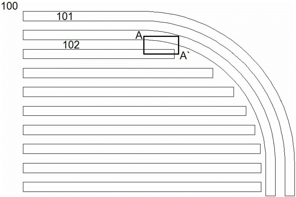
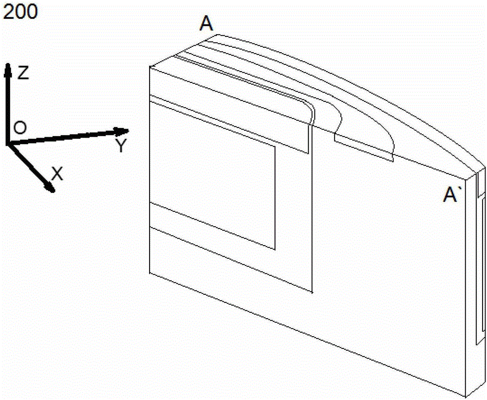
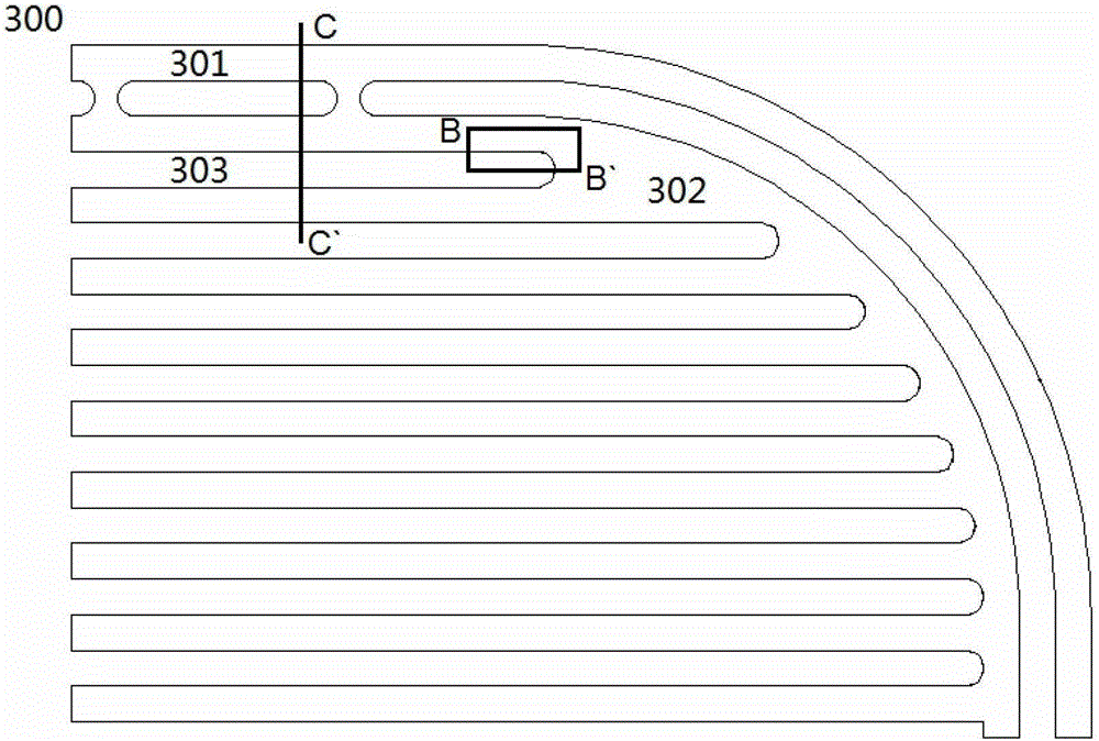
[0019] The present invention will be further described below in conjunction with accompanying drawing:
[0020] The present invention proposes layout edge design of split-gate trench power MOS devices. The trench structure in the device cell is specially designed to communicate with the terminal structure, and the mesa structure in the active region is a long strip structure with equal diameters and semicircles at both ends. While not adding process steps and photolithographic plates, the process steps are saved, the breakdown voltage of the device is ensured, and the working reliability of the device is improved.
[0021] In the research of split-gate trench power MOS devices, it is found that when the trench depth is constant, the breakdown voltage of split-gate trench power MOS devices is mainly affected by the distance between the trenches in the active region of the device. The traditional split-gate MOS device has a trench structure surrounded by mesas. At the corner of ...
PUM
 Abstract
Description
Claims
Application Information
 - R&D Engineer
- R&D Manager
- IP Professional
- Industry Leading Data Capabilities
- Powerful AI technology
- Patent DNA Extraction
Browse by: Latest US Patents, China's latest patents, Technical Efficacy Thesaurus, Application Domain, Technology Topic, Popular Technical Reports.
© 2024 PatSnap. All rights reserved.Legal|Privacy policy|Modern Slavery Act Transparency Statement|Sitemap|About US| Contact US: help@patsnap.com