Eureka AIR delivers breakthrough ideas for toughest innovation challenges, trusted by R&D personnel around the world.

Insulated gate bipolar transistor structure integrated with Schottky diode and preparation method thereof

A technology of Schottky diodes and bipolar transistors, applied in semiconductor/solid-state device manufacturing, semiconductor devices, electrical components, etc., can solve the problems of increased switching power consumption, slow switching speed of devices, and long reverse recovery time, etc. Achieve the effects of increased switching speed, reduced switching power consumption, and reduced reverse recovery time

Active Publication Date: 2013-02-13
SHANGHAI HUAHONG GRACE SEMICON MFG CORP
View PDF3 Cites 4 Cited by
  • Summary
  • Abstract
  • Description
  • Claims
  • Application Information

AI Technical Summary

Problems solved by technology

[0003] However, since this bipolar transistor structure is dominated by minority carriers (referred to as minority carriers), when the device is turned off, the minority carrier reverse recovery time is long, which makes the switching speed of the device slower and the switching power consumption increases.
[0004] In addition, compared with the power MOS, the existing insulated gate bipolar transistor has a disadvantage that there is no inherent parasitic anti-parallel diode, which makes it must be used in some applications (such as inverters) with a freewheeling Diodes used in parallel

Method used


Image

  • Insulated gate bipolar transistor structure integrated with Schottky diode and preparation method thereof
  • Insulated gate bipolar transistor structure integrated with Schottky diode and preparation method thereof
  • Insulated gate bipolar transistor structure integrated with Schottky diode and preparation method thereof

Examples


Embodiment Construction

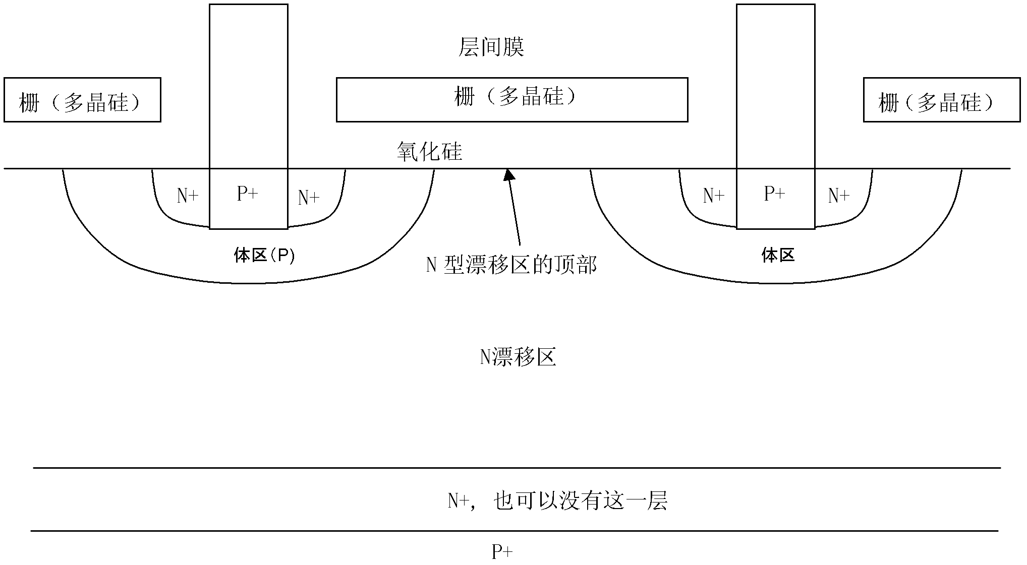
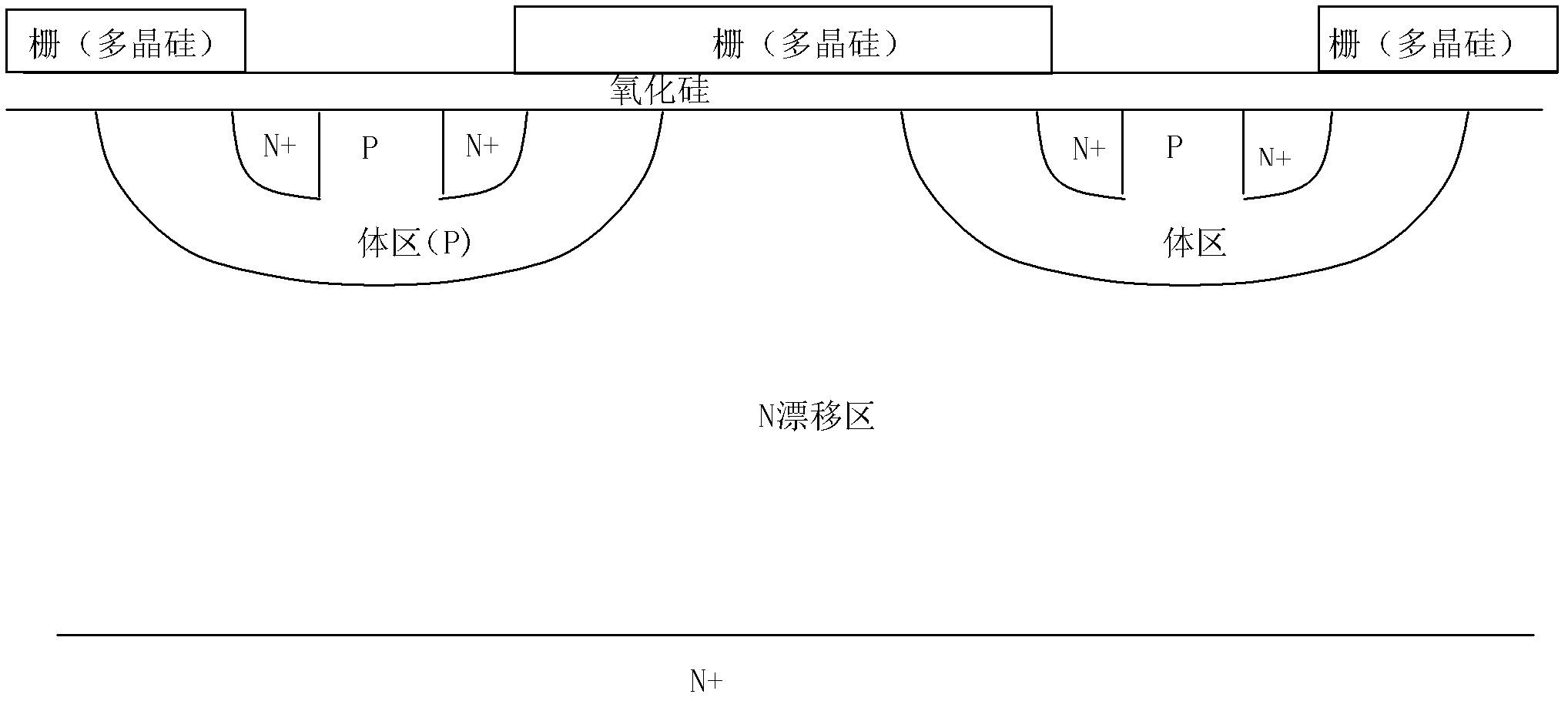
[0028] The structure of the insulated gate bipolar transistor integrated with the Schottky diode of the present invention is as follows figure 2 shown (the front metal on the contact top and the back metal on the lower part of the substrate are not shown), including an IGBT, the top of the N-type drift region of the IGBT includes the area covered by the polysilicon gate and the area not covered by the polysilicon The area covered by the gate (the area not covered by the polysilicon gate is set between two areas covered by the polysilicon gate); the area not covered by the polysilicon gate forms a Schottky contact with the metal above it, so that the Schottky diode and the insulated gate The bipolar transistors are integrated together to form a parallel relationship with the insulated gate bipolar transistors; the anode of the Schottky diode is connected to the emitter of the IGBT through the front metal (that is, the Schottky contact at the top of the N-type drift region is co...


PUM


Abstract

The invention discloses an insulated gate bipolar transistor structure integrated with a Schottky diode. The insulated gate bipolar transistor structure comprises an IGBT (Insulated Gate Bipolar Transistor), wherein the top parts of N-type drift regions of the IGBT comprise regions covered by polysilicon gates and regions not covered by the polysilicon gates; the regions not covered by the polysilicon gates and metal arranged at the upper parts thereof form Schottky contact, so that a Schottky diode is integrated with the IGBT and are connected with a collecting electrode and an emitting electrode of the IGBT in parallel. According to the invention, the Schottky diode is integrated in the IGBT, when current of the IGBT is conducted from the emitting electrode to the collecting electrode, freewheeling function can be achieved, so that the switching speed is improved, and the switching power consumption is reduced; and when the conduction of current of the IGBT from the collecting electrode to the emitting electrode is turned off, a bypass can be additionally provided for reverse recovery of minority carriers, so that the reverse recovery time for freewheeling turn-off is greatly reduced and the switching speed is improved. The invention further discloses a method for preparing the insulated gate bipolar transistor structure integrated with the Schottky diode.

Description

technical field [0001] The invention relates to an insulated gate bipolar transistor structure, in particular to an insulated gate bipolar transistor structure integrated with Schottky diodes. The invention also relates to a preparation method of an insulated gate bipolar transistor structure integrated with a Schottky diode. Background technique [0002] An insulated gate bipolar transistor (IGBT for short) is a combination of a metal oxide semiconductor (MOS for short) and a bipolar transistor (also called a triode). Existing IGBTs such as figure 1 The top of the N-type drift region is fully covered by the polysilicon gate as shown (the front-side metal contacting the top and the back-side metal below the substrate are not shown). This structure is suitable for high withstand voltage and high power applications because the bipolar transistor has a very low saturation voltage when it is turned on with a large current. Compared with the power MOS, the power consumption of ...

Claims


Application Information

Patent Timeline
IPC IPC(8): H01L29/06H01L29/739H01L21/331
Inventor 金勤海陈正嵘徐俊杰
Owner SHANGHAI HUAHONG GRACE SEMICON MFG CORP
Why Eureka
Eureka Blog
Learn More