Wafer level packaging structure with large contact area and preparation method thereof

A wafer-level packaging and contact surface technology, which is applied in semiconductor/solid-state device manufacturing, semiconductor/solid-state device components, semiconductor devices, etc. Small size and other issues

Active Publication Date: 2013-02-13
ALPHA & OMEGA SEMICON INT LP
View PDF8 Cites 45 Cited by
  • Summary
  • Abstract
  • Description
  • Claims
  • Application Information

AI Technical Summary

Problems solved by technology

Among them, the solder balls or solder bumps planted on the wafer-level chip are used as the contact terminals for the electrical connection between the chip and the external circuit. As we all know, the power consumption of power devices is very large, and the solder balls or solder bumps are usually directly Soldered on the pads on the PCB printed circuit board, usually the volume of the solder balls or solder bumps is relatively small and their contact surface with the outside world is also very limited, which makes them easy to cause high impedance (High impedance) and Low thermal conductance effect
In addition, the exposed chip in the wafer-level chip size package not only lacks physical protection, which makes the chip easily damaged during transportation or various process preparation processes, but also such chips that are not resistant to moisture are also likely to reduce their service life

Method used


Image

  • Wafer level packaging structure with large contact area and preparation method thereof
  • Wafer level packaging structure with large contact area and preparation method thereof
  • Wafer level packaging structure with large contact area and preparation method thereof

Examples


Embodiment Construction

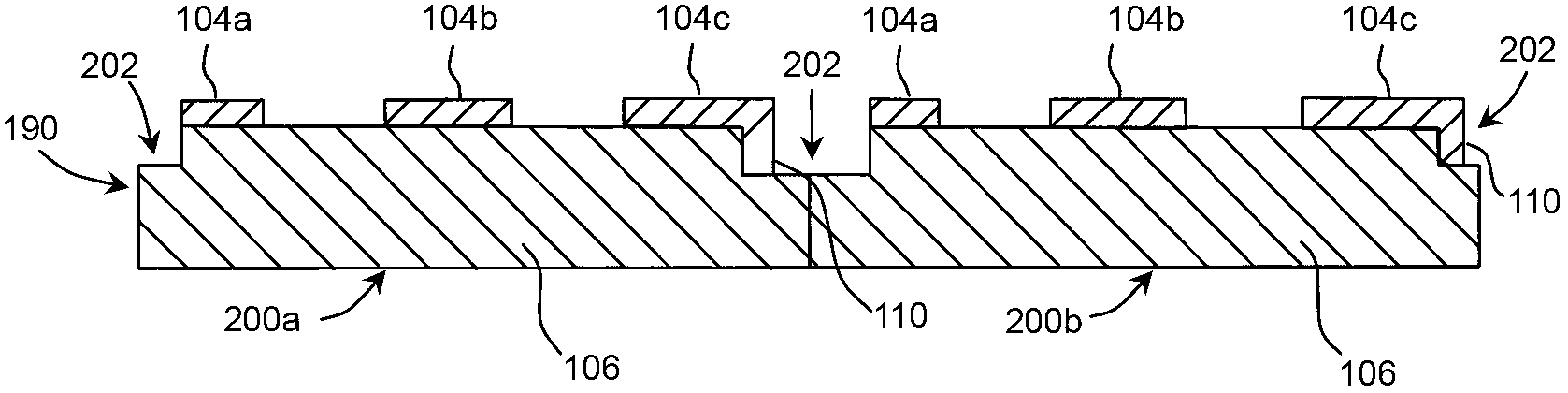
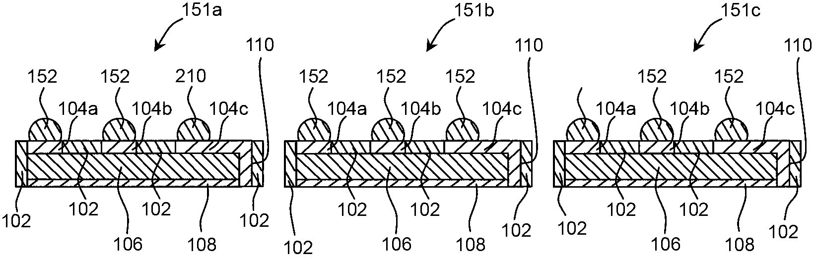
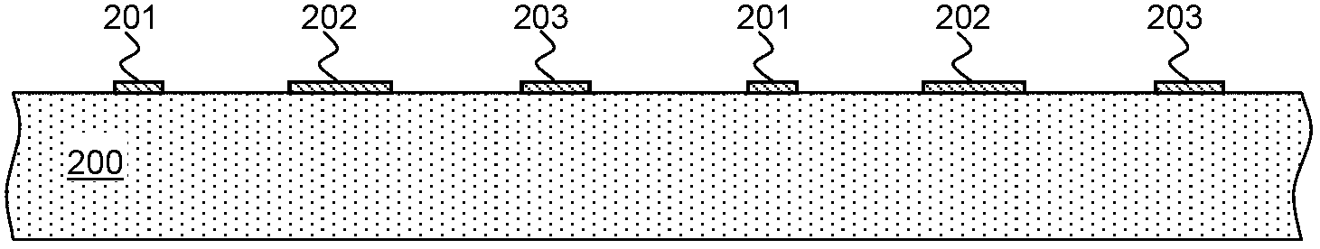
[0052] see Figure 2A , the wafer 200 usually contains a large number of chips connected together by casting, and the boundary between adjacent chips is defined by an unillustrated scribe line (Scribe line), and finally the chips can be removed from the wafer 200 along the scribe line. Cutting and separation, since these technical features are well known to those skilled in the art, the present invention is no longer Figure 2A Chips are intentionally marked additionally. Under known technical conditions, after the normal preparation process of the wafer 200 is completed, a plurality of first-type metal pads 201, 202 are usually prepared on the front side of the wafer 200. The front side of any one of the included chips is prepared with first-type metal pads 201 , 202 . The first type of metal pads 201, 202 are usually aluminum-silicon metal pads (I / O Pads) pre-designed on the chip, and the first type of metal pads 201, 202 are usually used as electrodes of the chip or with ...


PUM


Abstract

The present invention relates to a package for semiconductor device and the fabrication method for integrally encapsulating a whole semiconductor chip within a molding compound. In the semicondcutor device package, bonding pads distributed on the top of the chip are redistributed into an array of redistributed bonding pads located in an dielectric layer by utilizing the redistribution technique. The electrodes or signal terminals on the top of the semiconductor chip are connected to an electrode metal segment on the bottom of the chip by conductive materials filled in through holes formed in a silicon substrate of a semiconductor wafer. Furthermore, the top molding portion and the bottom molding portion seal the semiconductor chip completely, thus providing optimum mechanical and electrical protections.

Description

technical field [0001] The present invention generally relates to a method for preparing a wafer-level package. More specifically, the present invention aims to provide a wafer-level package structure and a preparation method with a relatively large soldering contact surface. Background technique [0002] Wafer Level Chip Scale Packaging (WLCSP) is a kind of IC packaging method. After the whole wafer is produced, the packaging test and ball planting are directly performed on the wafer, and then it is cut and made. For a single IC, the size of the chip that completes the packaging process is almost equal to the size of the original die. Among them, the solder balls or solder bumps planted on the wafer-level chip are used as the contact terminals for the electrical connection between the chip and the external circuit. As we all know, the power consumption of power devices is very large, and the solder balls or solder bumps are usually directly Soldered on the pads on the PCB ...

Claims


Application Information

Patent Timeline
Patent Type & Authority Applications(China)
IPC IPC(8): H01L21/48H01L21/768H01L23/488H01L23/538
CPCH01L2224/13009H01L23/3114H01L24/03H01L2221/68377H01L23/3135H01L21/76898H01L2224/13022H01L2224/05548H01L24/05H01L24/13H01L2924/13091H01L2224/13024H01L21/6836H01L2221/68359H01L2224/1184H01L2224/131H01L2221/6834H01L23/481H01L24/11H01L2224/94H01L21/561H01L2224/05571H01L2224/02166H01L2224/0401H01L2224/05554H01L2924/00014H01L2924/12042H01L2924/1306H01L2924/181H01L2224/03H01L2224/11H01L2924/00012H01L2924/014H01L2924/00H01L2224/05552
Inventor 薛彦迅
Owner ALPHA & OMEGA SEMICON INT LP
Why Eureka
Try Eureka