


Quick Research
Generate reliable direction feasibility study reports for your R&D in just a few steps.

Technical Q&A
Discover and master advanced knowledge NOW. Basics, ideas, possibilities, all at once.

Find Solutions
As an expert in R&D theories, this can generate solutions to your technical problems instantly.

Evaluate Feasibility
Analyze your overall solution with one click, know your potential R&D risks in advance.

Monitor Landscape
Get weekly tech updates, stay abreast of the latest tech innovations and key insights.
Light emitting device and method for manufacturing the same
A technology for a light-emitting device and a manufacturing method, which are applied to electrical components, electrical solid-state devices, circuits, etc., can solve problems such as reduction in the amount of light beams, and achieve the effects of improving extraction efficiency, realizing miniaturization, and suppressing deterioration of optical properties.
- Summary
- Abstract
- Description
- Claims
- Application Information
AI Technical Summary
Problems solved by technology
Method used
Image

Examples
Embodiment approach 1
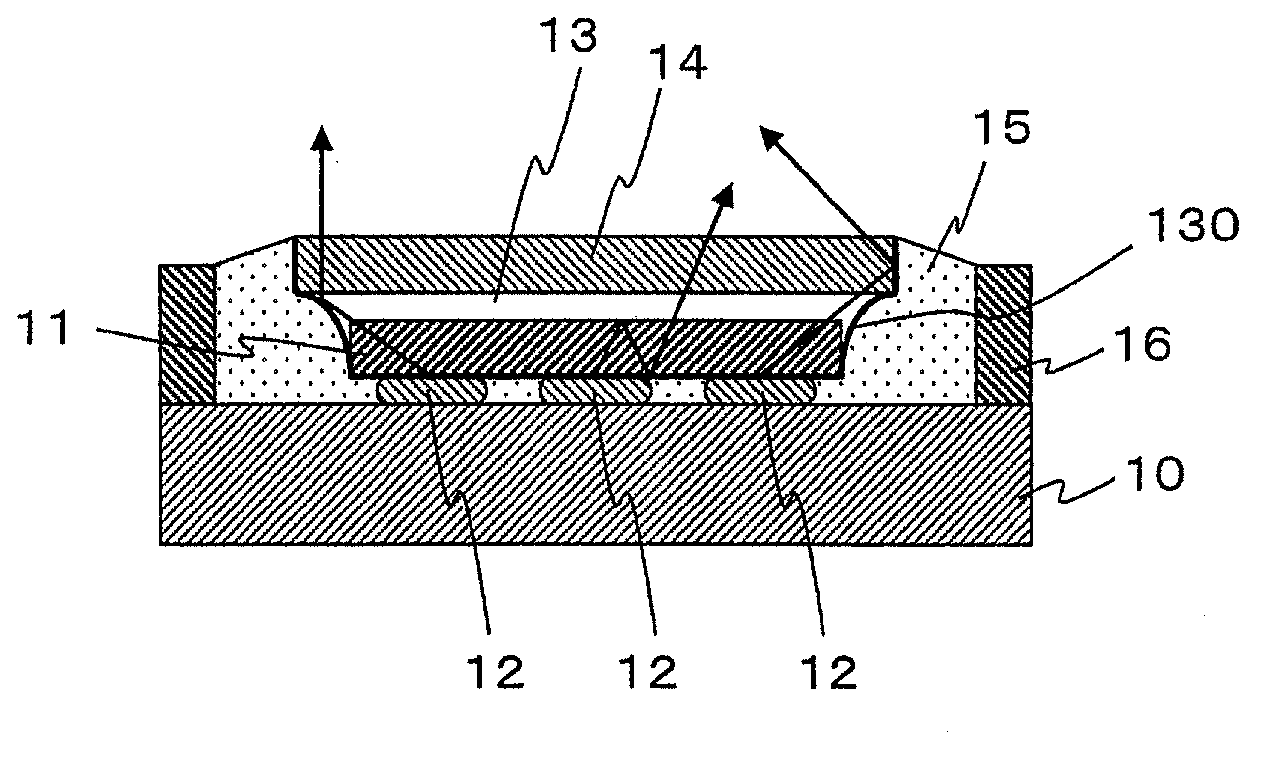
[0042] figure 1 A cross-sectional view of the light emitting device according to Embodiment 1 is shown. This light emitting device includes a reflective surface (inclined surface) 130 for light extraction at a position close to the side surface of the light emitting element 11 .
[0043] Specifically, a flip-chip light emitting element 11 is mounted on a submount substrate 10 on which wiring is formed on the upper surface by bonding with a plurality of bumps 12 . A resin layer 13 transparent to the light emitted by the light emitting element 11 is mounted on the upper surface of the light emitting element 11 , and a plate-shaped member 14 having a wavelength conversion function is mounted on the resin layer 13 .
[0044] A frame 16 is disposed outside the light emitting element 11 , and the space between the light emitting element 11 and the frame 16 is filled with the reflective material layer 15 . The reflective material layer 15 uses a non-conductive material with high re...
Embodiment approach 2
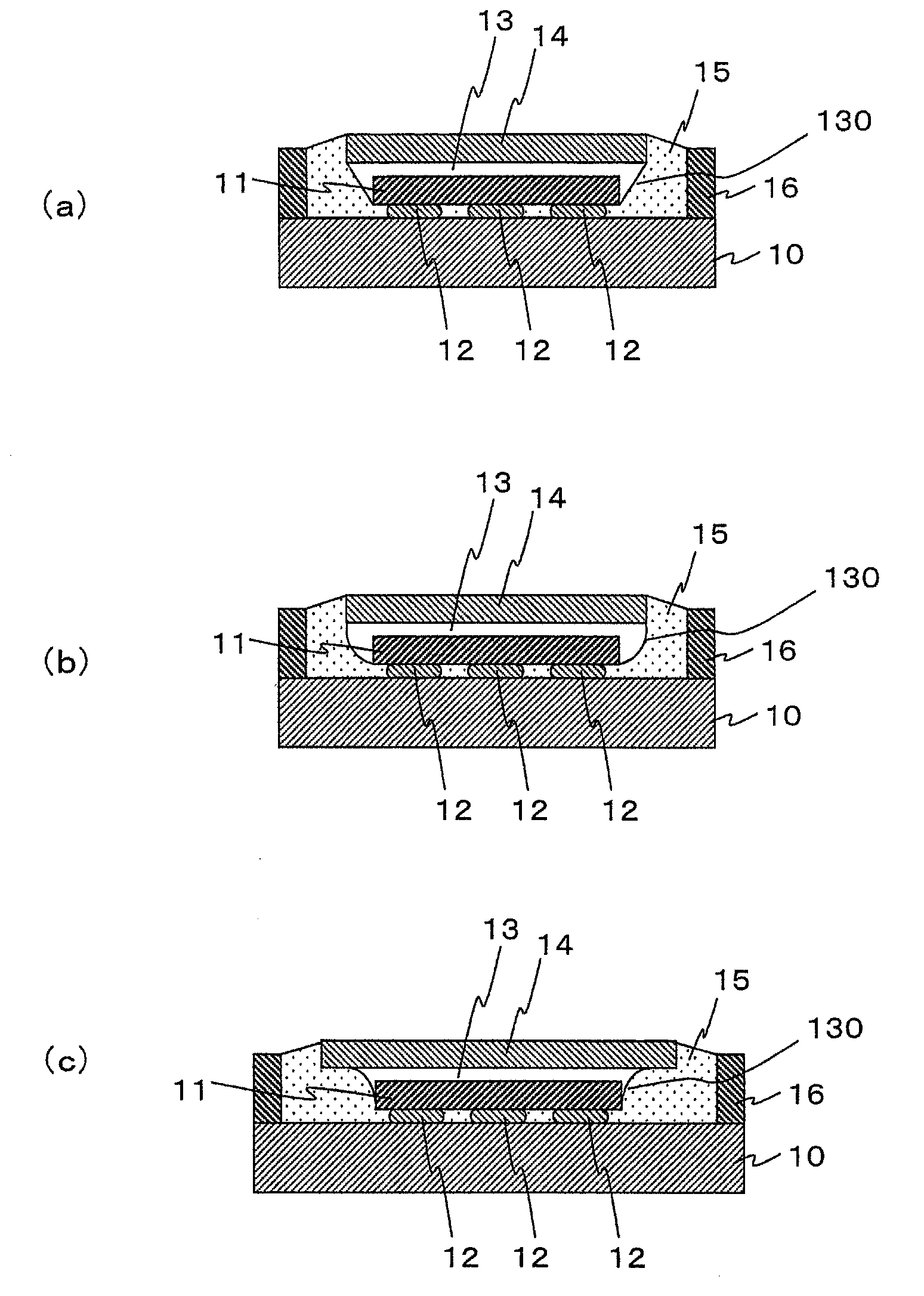
[0074] Next, as Embodiment 2, a light emitting device in which a plurality of light emitting elements 11 are mounted on one submount substrate 10 will be described. Figure 6 (a), (b), and (c) show cross-sectional views of the light emitting device of Embodiment 2. FIG.
[0075] A plurality of light emitting elements 11 are covered with one plate member 14 . A reflective material layer 15 surrounding a plurality of light emitting elements 11 is arranged. The inclined surface 130 on the side of the resin layer 13 is preferably an inclined surface that linearly connects the bottom surface of the light emitting element 11 and the lower surface of the plate member 14, or is Figure 6 Curved surfaces convex toward the light emitting element 11 side as in (a) to (c). Particularly preferred is a convex curved surface with a curvature of 5 or less.
[0076] Such as Figure 6 As shown in (a) and (b), the surface of the resin layer 13 is a curved surface that is convex toward the pl...
Embodiment approach 3
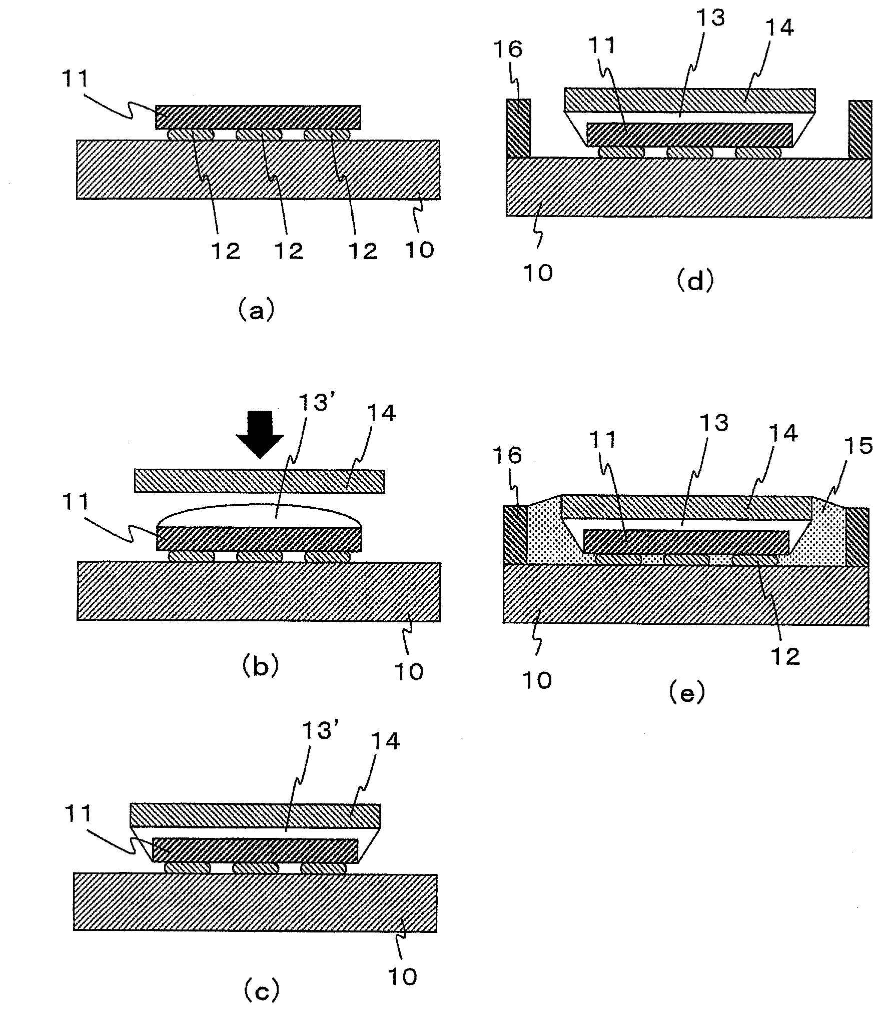
[0094] Figure 9 (a) shows a cross-sectional view of a light emitting device according to Embodiment 3, Figure 9 (b) and (c) are top views. Such as Figure 9 As shown in (a), a flip-chip type light emitting element 11 is mounted on a submount substrate 10 having wiring formed on the upper surface by bonding with a plurality of bumps 12 . A resin layer 13 having a wavelength conversion function is mounted on the upper surface of the light emitting element 11 , and a transparent plate-shaped member 14 is mounted on the resin layer 13 .
[0095]In the base material of the resin layer 13, phosphor particles 13a are dispersed at a high concentration, and spacers 13b are also dispersed. As the base material, a material transparent to the light emitted by the light emitting element 11 and the fluorescence emitted by the phosphor particles 13 a excited by the light emitted by the light emitting element 11 is used. As for the base material, a transparent resin is used in the same ...
PUM
 Abstract
Description
Claims
Application Information
 - R&D Engineer
- R&D Manager
- IP Professional
- Industry Leading Data Capabilities
- Powerful AI technology
- Patent DNA Extraction
Browse by: Latest US Patents, China's latest patents, Technical Efficacy Thesaurus, Application Domain, Technology Topic, Popular Technical Reports.
© 2024 PatSnap. All rights reserved.Legal|Privacy policy|Modern Slavery Act Transparency Statement|Sitemap|About US| Contact US: help@patsnap.com