
Polishing reagent liquid composition for semiconductor chip, polishing reagent liquid and preparation method thereof

A composition and semiconductor technology, which is applied in the fields of polishing compositions containing abrasives, semiconductor/solid-state device manufacturing, electrical components, etc., can solve the problems of inability to obtain good mirror effect and high cost of polishing liquid, and achieve the guarantee of wafer Surface quality, high-quality mirror effect, good polishing effect

Inactive Publication Date: 2013-01-30
BEIJING TONGMEI XTAL TECH CO LTD
View PDF4 Cites 0 Cited by
  • Summary
  • Abstract
  • Description
  • Claims
  • Application Information

AI Technical Summary

Problems solved by technology

[0005] In order to overcome the defects that the existing polishing liquid cannot obtain a good mirror effect when polishing a semiconductor wafer with a special angle, corrosion pits and holes are prone to appear on the surface of the wafer, and the cost of the polishing liquid is high. Composition for semiconductor wafer polishing liquid

Method used


Image

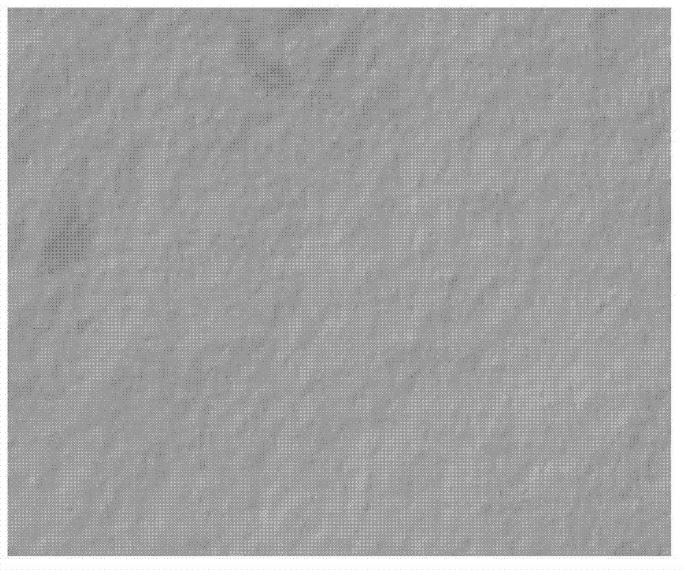
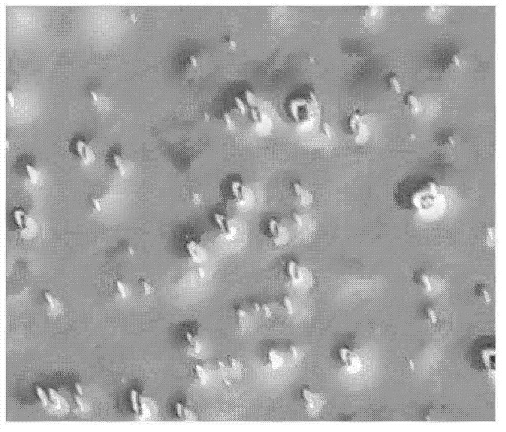
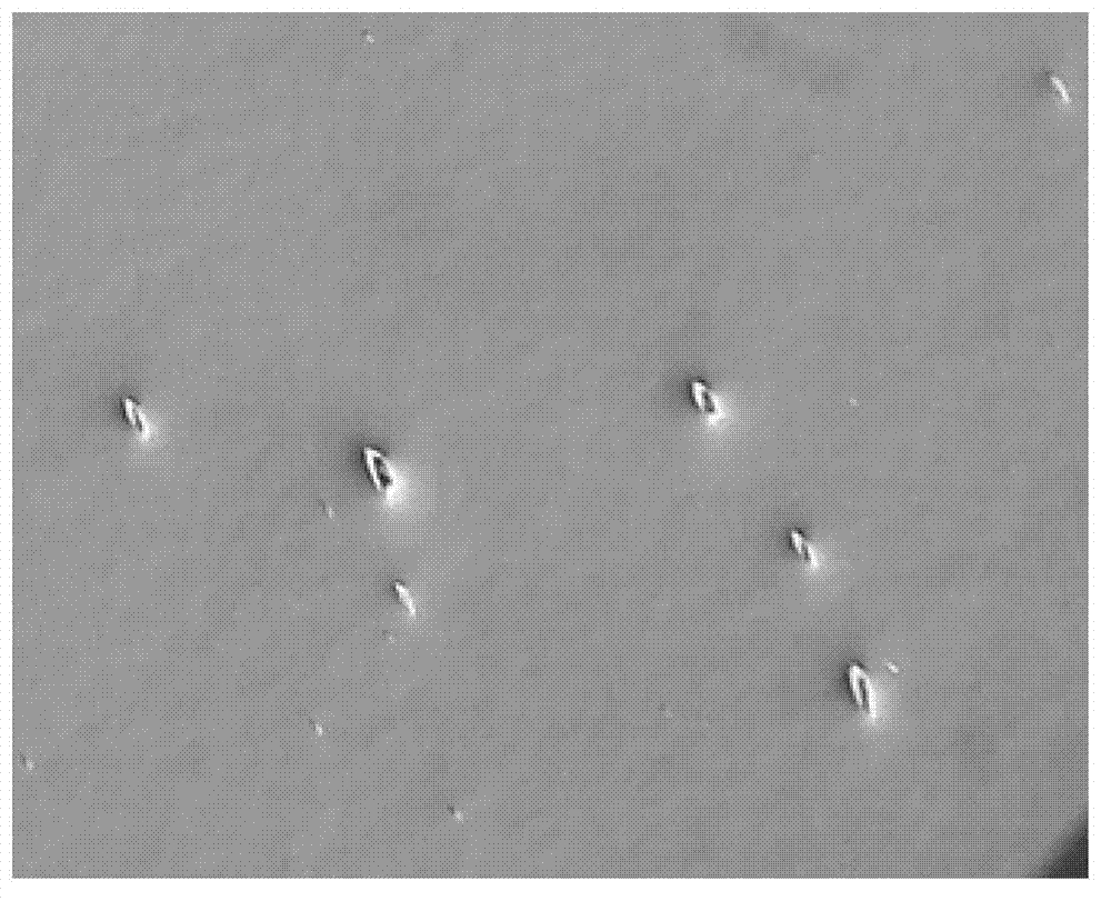
  • Polishing reagent liquid composition for semiconductor chip, polishing reagent liquid and preparation method thereof
  • Polishing reagent liquid composition for semiconductor chip, polishing reagent liquid and preparation method thereof
  • Polishing reagent liquid composition for semiconductor chip, polishing reagent liquid and preparation method thereof

Examples


Embodiment 1

[0040] 1. The configuration of polishing liquid

[0041] 1. Proportion of liquid medicine

[0042] Lithium hypochlorite: 1000 g; sodium bicarbonate: 350 g; silica sol: 2 liters (Tianjin Xilika, SiO 2 The concentration is about 30wt%, SiO 2 The particle size is 80-120nm and the specific gravity is about 1.28).

[0043] 2. Liquid medicine preparation process

[0044] (1) Add 70 liters of deionized water at 10-19°C into a 100-liter dispensing barrel.

[0045] (2) Start stirring and slowly pour 1000g of lithium hypochlorite and stir for 5 minutes.

[0046] (3) Pour 350 g of sodium bicarbonate while stirring continuously, and continue stirring for 20 minutes.

[0047] (4) Add 2L of silica sol, then add tap water to the 100L mark, stir for 5 minutes, and the preparation is complete.

[0048] 2. Wafer polishing

[0049] Polishing machine: choose 9B-5P double-sided polishing machine produced by SPEED FAM Company 1, loading

[0050] Place the gallium arsenide wafer to be polished in the planetary whe...

Embodiment 2

[0063] 1. The configuration of polishing liquid

[0064] 1. Proportion of liquid medicine

[0065] Lithium hypochlorite: 1200g; Potassium bicarbonate: 500g; Silica sol: 2.5L (Tianjin Jingling, SiO 2 The concentration is about 40wt%, SiO 2 The particle size is 80-120nm and the specific gravity is about 1.32).

[0066] 2. Liquid medicine preparation process

[0067] (1) Add 70 liters of deionized water at 10-19°C into a 100-liter dispensing barrel.

[0068] (2) Start stirring and slowly pour 1200g lithium hypochlorite, and stir for 5 minutes.

[0069] (3) Pour 500g of potassium bicarbonate under constant stirring, and continue stirring for 20 minutes.

[0070] (4) Add 2.5L of silica sol, then add tap water to the 100L mark, stir for 5 minutes, and the preparation is complete.

[0071] 2. Wafer polishing

[0072] Polishing machine: choose 9B-5P double-sided polishing machine produced by SPEED FAM

[0073] 1. Loading

[0074] Place the InP wafer to be polished in the planetary wheel hole in the p...


PUM

PropertyMeasurementUnit
particle diameteraaaaaaaaaa
lengthaaaaaaaaaa

Abstract

The invention relates to a polishing reagent liquid composition for a semiconductor chip. The polishing reagent liquid composition comprises lithium hypochlorite, bicarbonate and silica sol. The invention also relates to a polishing reagent liquid containing the composition and a preparation method thereof. The polishing reagent liquid provided by the invention is directed at a semiconductor chip with a special angle and allows an excellent smooth and uniform chip surface without defects like etch pits and holes to be obtained. According to the invention, the polishing reagent liquid can be used as a universal polishing reagent liquid; raw materials for the polishing reagent liquid are cheap and easily available, so cost of the polishing reagent liquid is reduced; and the polishing reagent liquid has a wide market application value.

Description

Technical field [0001] The invention relates to the field of semiconductor materials, in particular to a polishing chemical composition for semiconductor wafers, a polishing chemical and a preparation method of the polishing chemical. Background technique [0002] Gallium arsenide (GaAs), Si and indium phosphide (InP) wafers are all commonly used semiconductor materials. Especially in recent years, the development of gallium arsenide wafers is very rapid. With its excellent performance, gallium arsenide wafers have gradually replaced Si wafers and become an ideal material in the semiconductor industry. The processing method of the gallium arsenide wafer is to first cut the gallium arsenide crystal into pieces with a metal saw or a wire saw, and then complete the processing process through processes such as grinding and mechanical chemical polishing. The cut surface of gallium arsenide wafers is usually (100), that is, the surface of the wafer is usually (100). However, in some s...

Claims


Application Information

Patent Timeline
Patent Type & Authority Applications(China)
IPC IPC(8): C09G1/02H01L21/304
Inventor 刘建志吴怀东刘文森赵波刘征
Owner BEIJING TONGMEI XTAL TECH CO LTD
Learn More