Device for rapid annealing of semiconductor silicone chip

A rapid annealing, semiconductor technology, applied in crystal growth, post-processing details, post-processing and other directions, can solve problems such as affecting the recovery of silicon single crystals to the true resistivity, and achieve strong industrial operability, high efficiency, and simple structure. Effect

Active Publication Date: 2015-02-11
ZHEJIANG COWIN ELECTRONICS
View PDF4 Cites 0 Cited by
  • Summary
  • Abstract
  • Description
  • Claims
  • Application Information

AI Technical Summary

Problems solved by technology

If the temperature range of 350~500℃ cannot be jumped quickly, thermal donors will be re-formed, affecting the recovery of silicon single crystals to the true resistivity

Method used


Image

  • Device for rapid annealing of semiconductor silicone chip

Examples


Embodiment Construction

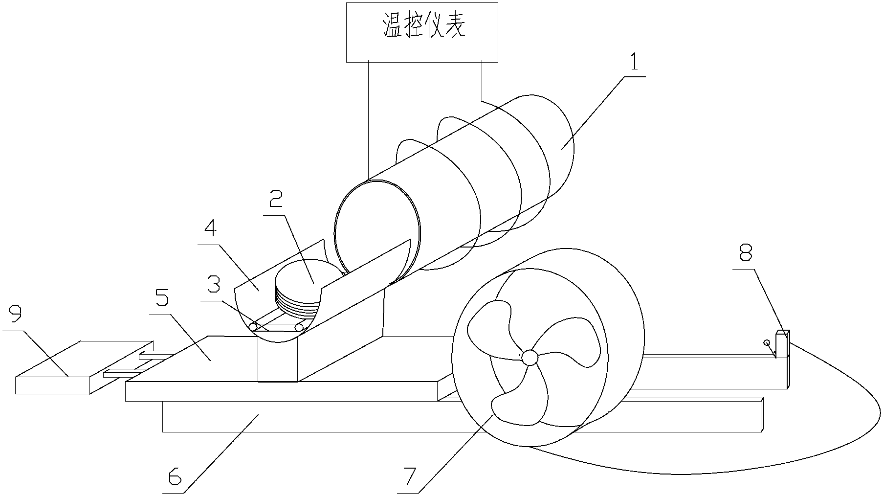
[0023] Combine below figure 1 Specifically illustrate an embodiment of a device for rapid annealing of semiconductor silicon wafers of the present invention, comprising a support bracket 4 that receives the semiconductor silicon wafer 2 from the heat treatment furnace 1, a mobile slide 5 fixedly connected to the support bracket 4, and cooperating with the mobile slide 5 The sliding guide rail 6, the device also includes a contact switch 8 located on the sliding guide rail and the cooling fan 7 controlled by the contact switch. The contact switch controls the cooling fan to be turned on, and the mobile slide plate 5 is driven by the drive mechanism to slide on the sliding guide rail. Described driving mechanism is an air cylinder 9, and this air cylinder is closed by the control of contact switch 8.

[0024] The support bracket is a plate with an arc-shaped cross section, and the support bracket has the same radian as the lower half of the furnace mouth of the heat treatment f...


PUM


Abstract

The invention discloses a device for the rapid annealing of a semiconductor silicone chip, which comprises a supporting bracket used for bearing a semiconductor silicone chip coming out of a thermal treatment furnace, a movable sliding plate fixedly connected with the supporting bracket, a sliding guide rail matched with the movable sliding plate, a contacting type switch arranged on the sliding guide rail and a cooling fan turned off or on by the contacting type switch. When the semiconductor silicone chip moves to the air flow middle part of the cooling fan along with the movable sliding plate, the contacting type switch controls the on-off state of the cooling fan, and the movable sliding plate is driven by a driving mechanism to slide on the sliding guide rail. The device for the rapid annealing of the semiconductor silicone chip can effectively realize rapid annealing and be used for the thermal processing annealing section in the actual processing and manufacturing processes of the semiconductor silicone chip, and has the advantages of simplicity in structure, convenience in operation and high efficiency.

Description

technical field [0001] The invention belongs to the field of semiconductor silicon wafer manufacturing and processing, and relates to a rapid annealing device suitable for the heat treatment process of semiconductor silicon wafers. Background technique [0002] Czochralski silicon single crystal is to place polysilicon in a high-purity quartz crucible and melt it at high temperature, because the high-purity crucible is in direct contact with molten silicon and is at a high temperature above 1450 degrees Celsius. At high temperature, SiO2 will react with molten silicon to grow SiO and partially dissolve in In molten silicon, as the crystal grows into the interior of the crystal, oxygen in silicon is formed. [0003] At the same time, the growth of direct silicon single crystal is slowly solidified and grown from a high-temperature melt, and the driving force of crystal growth mainly comes from the supercooling degree formed by the temperature gradient, so a period of thermal ...

Claims


Application Information

Patent Timeline
Patent Type & Authority Patents(China)
IPC IPC(8): C30B33/02
Inventor 孙新利万喜增蒋伟达郑六奎
Owner ZHEJIANG COWIN ELECTRONICS
Why Eureka
Try Eureka