Coreless package substrate and fabrication method thereof

一种封装基板、无核心层的技术,应用在半导体/固态器件制造、电路、电固体器件等方向,能够解决第二电性接触垫123间距无法细间距化、面积缩小、芯片易脱落等问题

Active Publication Date: 2013-01-09
UNIMICRON TECH CORP
View PDF3 Cites 12 Cited by
  • Summary
  • Abstract
  • Description
  • Claims
  • Application Information

AI Technical Summary

Problems solved by technology

[0005] However, in the existing packaging substrate 1, the openings 140a, 140b need to be formed on the solder resist layers 14a, 14b, and the alignment between the solder balls 15a, 15b and the openings 140a, 140b is not easy, thus increasing the difficulty of the process.
[0006] In addition, the opening 140b of the solder resist layer 14b only exposes part of the top surface of the second electrical contact pad 123 instead of exposing the entire top surface, so that the area of ​​the top surface of the metal bump 13b is reduced, resulting in subsequent When the chip is connected, the bonding force between the metal bump 13b and the chip is reduced, so that the chip is easy to fall off and be damaged
[0007] In addition, in order to avoid the connection between the upper side solder balls 15b and produce a short circuit, and the size of the opening 140b of the solder resist layer 14b needs to be considered to maintain the bonding force of the metal bump 13b, so each of the second electrical properties The distance between the contact pads 123 needs to be increased, so that the pitch of the second electrical contact pads 123 cannot be finer, making it difficult to increase the layout density of the second electrical contact pads 123

Method used


Image

  • Coreless package substrate and fabrication method thereof
  • Coreless package substrate and fabrication method thereof
  • Coreless package substrate and fabrication method thereof

Examples


Embodiment Construction

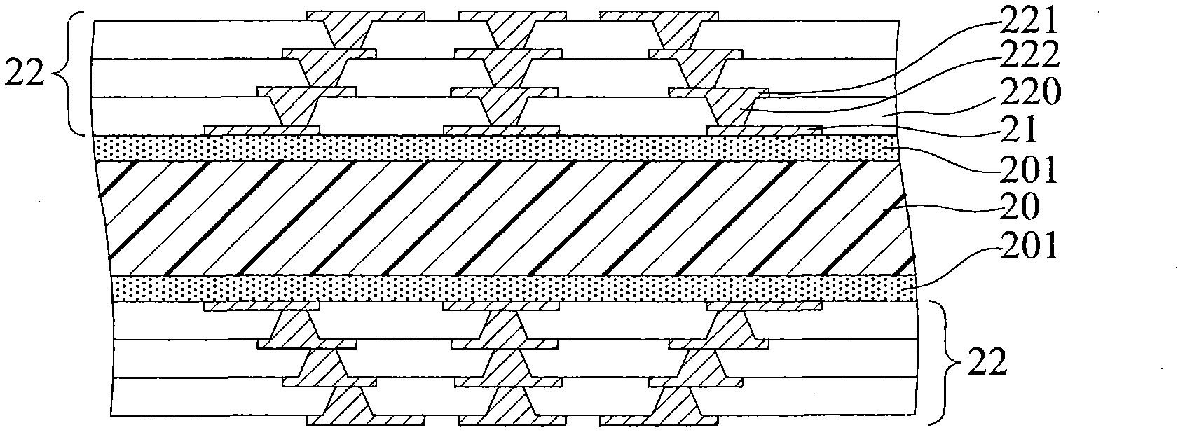
[0047] The implementation of the present invention will be described below through specific examples, and those skilled in the art can easily understand other advantages and effects of the present invention from the content disclosed in this specification.

[0048] It should be noted that the structures, proportions, sizes, etc. shown in the drawings attached to this specification are only used to match the content disclosed in the specification, for the understanding and reading of those familiar with this technology, and are not used to limit the implementation of the present invention Therefore, it has no technical substantive meaning. Any modification of structure, change of proportional relationship or adjustment of size shall still fall within the scope of this invention without affecting the effect and purpose of the present invention. The technical content disclosed by the invention must be within the scope covered. At the same time, terms such as "above", "below", "ab...


PUM


Abstract

A coreless package substrate is provided, including: a circuit buildup structure including at least a dielectric layer, at least a circuit layer and conductive elements; first electrical contact pads embedded in the lowermost dielectric layer of the circuit buildup structure; a plurality of metal bumps formed on the uppermost circuit layer of the circuit buildup structure; a dielectric passivation layer disposed on a top surface of the circuit buildup structure and the metal bumps; and second electrical contact pads embedded in the dielectric passivation layer and electrically connected to the metal bumps. With the second electrical contact pads being engaged with the metal bumps and having top surfaces thereof completely exposed, the bonding strength between the second electrical contact pads and a chip to be mounted thereon and between the second electrical contact pads and the metal bumps can be enhanced.

Description

technical field [0001] The present invention relates to a packaging substrate, in particular to a coreless packaging substrate and a manufacturing method thereof. Background technique [0002] With the vigorous development of the electronic industry, electronic products are gradually moving towards the trend of multi-function and high performance. At present, different packaging types have been developed for the semiconductor packaging structure, such as: wire bonded or flip-chip, in which a semiconductor chip is placed on a package substrate, and the semiconductor chip is electrically connected to the package by wires or solder bumps on the substrate. In order to meet the packaging requirements of high integration and miniaturization of semiconductor packages for more active and passive components and wiring, the packaging substrate has gradually evolved from a double-layer circuit board to a multi-layer circuit board ( multi-layer board), to use interlayer connection tec...

Claims


Application Information

Patent Timeline
Patent Type & Authority Applications(China)
IPC IPC(8): H01L23/488H01L23/00H01L21/60H01L21/48
CPCH01L2924/15311H01L21/4857H01L2224/16237H01L21/48H01L2224/73204H01L2224/32225H01L21/4846H01L2224/131H01L23/00H01L23/49822H01L23/488H01L2224/16225H01L23/3128H05K1/111H01L24/16H01L2924/12042Y10T29/49124Y10T29/49155H01L2924/00H01L2924/014
Inventor 曾子章何崇文
Owner UNIMICRON TECH CORP
Why Eureka
Try Eureka