Production process for O.J diode
A production process and diode technology, which is applied in the field of O.J diode production process, can solve the problems of product electrical degradation, thermal breakdown, and copper atoms cannot be cleaned thoroughly, so as to save resources and avoid electrical degradation.
- Summary
- Abstract
- Description
- Claims
- Application Information
AI Technical Summary
Problems solved by technology
Method used
Image
Examples
Embodiment Construction
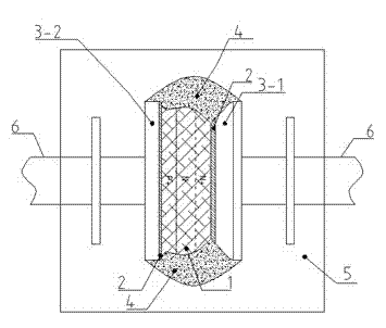
[0016] figure 1 A schematic diagram of the O.J diode structure is shown, which includes a chip 1. The two ends of the chip 1 are welded with solder 2. The lead near the P+ end of the chip is a flat lead 3-2, and the lead connected to the N+ surface of the chip is a tapered lead. 3-1, apply glue 4 on the chip 1 and the end of the lead, encapsulate the chip 1 and the lead with epoxy resin 5 , and provide an electroplating layer 6 on the periphery of the lead.
[0017] The O.J diode key process step of making above-mentioned structure among the present invention is as follows:
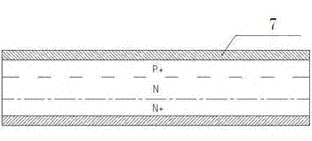
[0018] Coating photoresist: such as figure 2 As shown, after nickel plating is completed on the P+ and N+ surfaces of the silicon wafer, the photoresist 7 is coated on the P+ and N+ surfaces of the silicon wafer to protect the electrode surface during the corrosion process. The thickness of the photoresist is 100~300um.
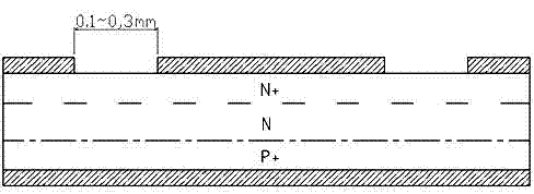
[0019] Lithography: such as image 3 As shown, the N+ surface is photolithograph...
PUM
 Abstract
Description
Claims
Application Information
 - Generate Ideas
- Intellectual Property
- Life Sciences
- Materials
- Tech Scout
- Unparalleled Data Quality
- Higher Quality Content
- 60% Fewer Hallucinations
Browse by: Latest US Patents, China's latest patents, Technical Efficacy Thesaurus, Application Domain, Technology Topic, Popular Technical Reports.
© 2025 PatSnap. All rights reserved.Legal|Privacy policy|Modern Slavery Act Transparency Statement|Sitemap|About US| Contact US: help@patsnap.com


