Eureka AIR delivers breakthrough ideas for toughest innovation challenges, trusted by R&D personnel around the world.

Preparation method of nanocrystalline Cu2O films

A nanocrystalline and thin film technology, applied in the field of semiconductors, can solve the problem of low photoelectric conversion efficiency

Inactive Publication Date: 2015-01-07
ANHUI UNIVERSITY OF ARCHITECTURE
View PDF1 Cites 0 Cited by
  • Summary
  • Abstract
  • Description
  • Claims
  • Application Information

AI Technical Summary

Problems solved by technology

Among new energy sources such as wind energy, ocean energy, solar energy, geothermal energy, and hydrogen energy, solar energy accounts for as much as 90%, constituting the absolute power of the new energy industry, but so far its photoelectric conversion efficiency is low

Method used


Image

  • Preparation method of nanocrystalline Cu2O films
  • Preparation method of nanocrystalline Cu2O films
  • Preparation method of nanocrystalline Cu2O films

Examples


Embodiment Construction

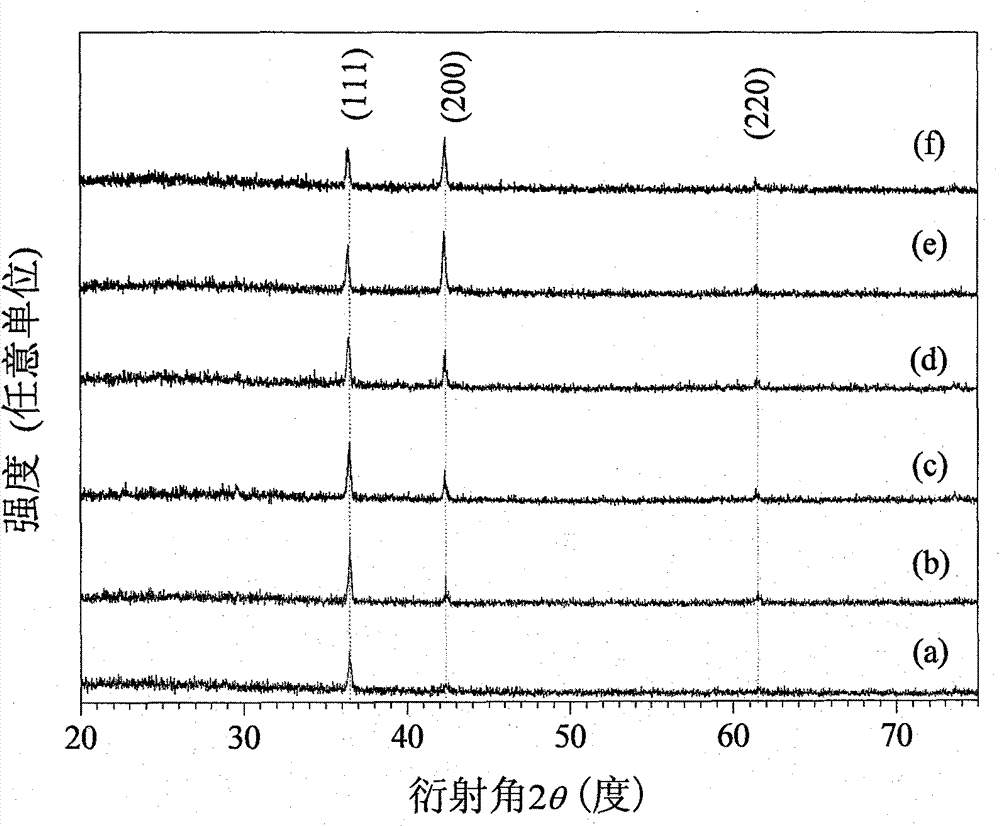
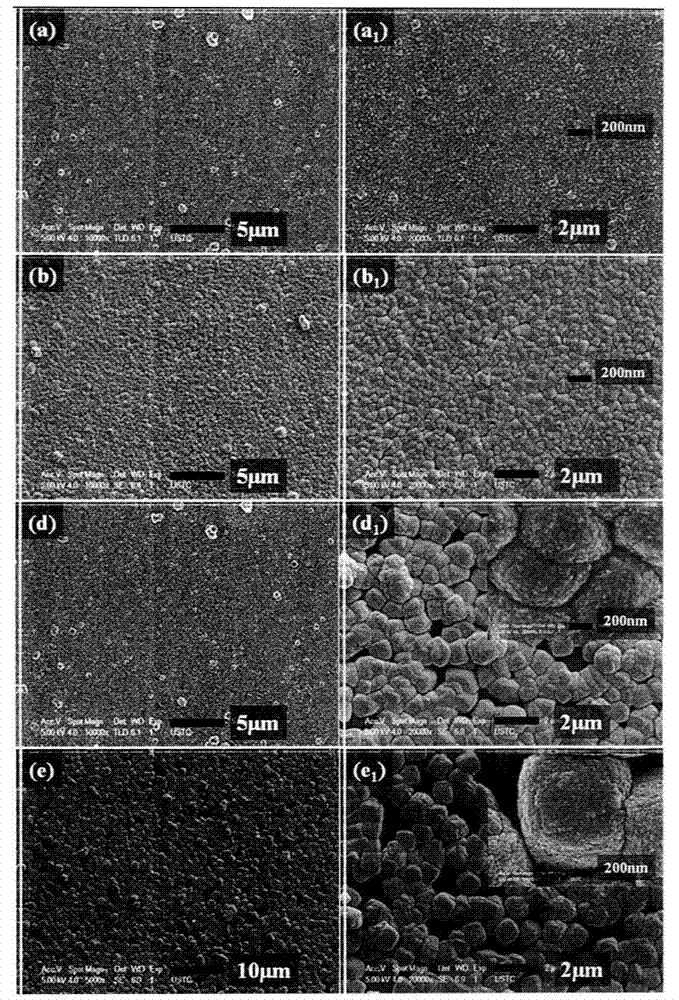
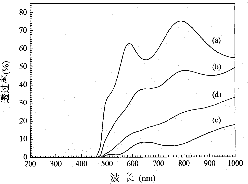
[0020] 1. According to the concentration ratio of 12:8:6, add the prepared sodium ascorbate and trisodium citrate solution in turn into the 0.8mol / L copper sulfate solution, stir evenly, and put it into the pre-cleaned and activated substrate after the complexation is sufficient. Make the volume of the solution 50ml, adjust the pH value of the solution to 8.8, react in a water bath at 80°C for 2 hours, take it out and clean it to get Cu 2 O film (a).

[0021] 2. According to the concentration ratio of 12:12:6, add the prepared sodium ascorbate and trisodium citrate solution in turn into the 0.8mol / L copper sulfate solution, stir evenly, and put it into the pre-cleaned and activated substrate after the complexation is sufficient. Make the volume of the solution 50ml, adjust the pH value of the solution to 8.8, react in a water bath at 80°C for 2 hours, take it out and clean it to get Cu 2 O film (b).

[0022] 3. According to the concentration ratio of 12:16:6, add the prepare...


PUM


Abstract

The invention relates to a preparation method of nanocrystalline Cu2O films and belongs to the field of semiconductors. In the exiting method, the requirements on equipment are ordinarily higher, the more complicated procedure is needed, and finally, the cost is difficult to control, so the application range of the Cu2O films can be seriously influenced. The preparation method of the nanocrystalline Cu2O films is characterized by comprising the following steps that sodium ascorbate solution and trisodium citrate solution are respectively and sequentially added into copper sulfate solution according to the conditions that the range of the molar concentration ratio of copper sulfate to trisodium citrate is 12:8-12:36, and the molar range of copper sulfate to sodium ascorbate is 1:3-5:6, and the full complexing is carried out; the pH value of solution is regulated to 7.0 to 10.0; the materials are placed in the water bath with temperature being 50 DEG C to 95 DEG C for reaction for 1.0 to 3.0 hours; and after the reaction finishes, the flushing and the drying are carried out, and required products are obtained. The method adopts a simper chemical bath deposition method relative to methods such as an anodic oxidation method, a thermal oxidation method, a sputtering method and a chemical vapor deposition method, the preparation process is greatly simplified, and in addition, obtained products are uniform and compact.

Description

technical field [0001] A Preferential Orientation Growth of Nanocrystalline Cu 2 A method for preparing an O thin film belongs to the field of semiconductors. technical background [0002] Cuprous oxide (Cu 2 O) is one of the earliest semiconductor materials discovered, and has been recognized by more and more people for its low price and wide range of material sources. Cu 2 O is a P-type semiconductor that can be excited by visible light, and its forbidden band width is about 1.9-2.2eV. polycrystalline Cu 2 O has good stability and can be used repeatedly without being easily oxidized to Cu(II) and reduced to Cu; secondly, Cu 2 O is non-toxic, has good compatibility with the environment, and is readily available. Therefore, it is a semiconductor material with great application potential, and has potential applications in superconductors, hydrogen production, solar cells, and electrochromism. Especially on solar cells, its theoretical conversion efficiency can reach 18...

Claims


Application Information

Patent Timeline
Patent Type & Authority Patents(China)
IPC IPC(8): C23C18/16
Inventor 徐海燕董金矿陈琛
Owner ANHUI UNIVERSITY OF ARCHITECTURE
Why Eureka
Eureka Blog
Learn More