
Method for strengthening thin film in flexible thin film transistor manufacturing process

A flexible thin film and transistor technology, applied in the field of microelectronics, can solve the problems of film cracking, peeling off, and no IGZO-TFT electrical performance curve.

Inactive Publication Date: 2012-12-19
GUANGDONG SINODISPLAY TECH
View PDF2 Cites 3 Cited by
  • Summary
  • Abstract
  • Description
  • Claims
  • Application Information

AI Technical Summary

Problems solved by technology

When the deposition temperature is 270°C, the device not only does not show the electrical performance curve of IGZO-TFT, but the film will crack or fall off on the substrate

Method used


Image

  • Method for strengthening thin film in flexible thin film transistor manufacturing process
  • Method for strengthening thin film in flexible thin film transistor manufacturing process

Examples


Embodiment Construction

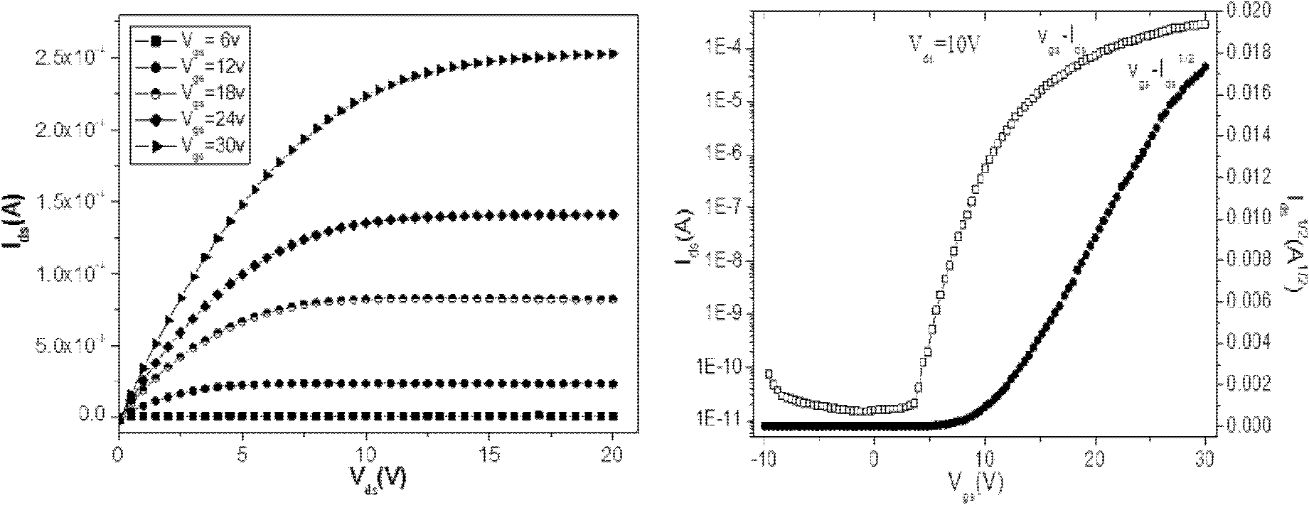
[0018] The method for preparing a process-enhanced thin film for a flexible thin film transistor provided by the present invention will be described in detail below with reference to the accompanying drawings and specific examples.

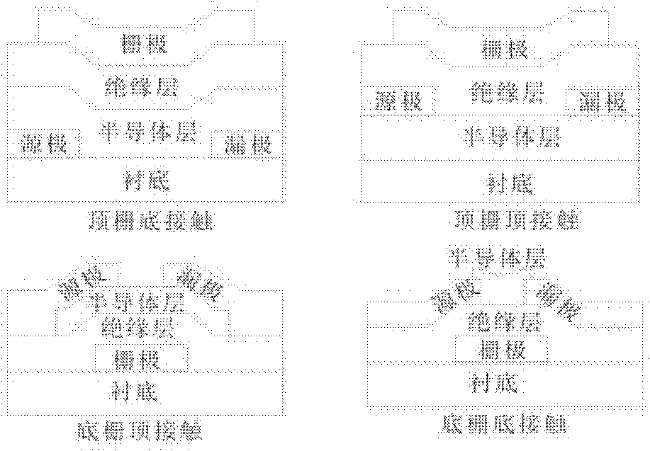
[0019] Fabrication of thin film layer of flexible IGZO-TFT device structure

[0020] Substrate Material Selection

[0021] The plastic substrate material of Dupont Company is selected, the model is Kapton E, and the specifications are 50 μm and 25 μm respectively, the former is used to prepare flexible devices, and the latter is used to explore the preparation of flexible transparent devices. It has a higher glass transition temperature (Tg=340°C), a lower thermal expansion coefficient (when the temperature is in the range of 50°C-200°C, the thermal expansion coefficient is 16ppm / °C), better chemical stability (unlike The solution in the prepared TFT reacts), good waterproof performance (for a 50μm thick Kapton E substrate, the water vapor permea...


PUM

PropertyMeasurementUnit
Deposition thicknessaaaaaaaaaa

Abstract

In order to overcome the defects in the prior art, the invention provides a method for strengthening the thin film transistor manufacturing process. The method comprises the steps of (1) lowering the highest deposition temperature; (2) reducing the deposition power of a protection layer; and (3) reducing the deposition thickness of a SiNx insulating layer. As the deposition temperature is reduced, and the deposition power of the protection layer and the thickness of a silicon nitride insulating layer are optimized, a flexible IGZO-TFT (Thin Film Transistor) device is manufactured successfully, the performances of the flexible IGZO-TFT are as follows: the threshold voltage is 8V, the switching ratio is 5*107, the saturated migration rate is 7.8cm2 / V.s, and the subthreshold slope factor is 0.9V / dec; the device is arranged on a cylinder with the curvature radius being 10mm is bent for 3 minutes, and the performances can not be changed basically; and the protection layer plays an important role in the stability of the device.

Description

technical field [0001] The invention relates to the technical field of microelectronics, and more particularly, to a method for strengthening a thin film of a thin film transistor (TFT). Background technique [0002] Thin film transistor refers to depositing a layer of semiconductor thin film on the substrate, and making the source, drain, gate and tube body through photolithography, etching and other technologies. It consists of gate insulating layer, active layer, gate electrode, The source and drain electrodes consist of several parts. figure 1 There are several common TFT structures, which can be divided into two categories: one is the top gate structure, also known as the normal staggered (NS for short) structure; the other is the bottom gate structure, also known as the inverted staggered (Inverted Staggered, Abbreviated as IS) structure. According to the different deposition sequences of the channel layer and the source-drain electrodes, the top-gate and bottom-gate...

Claims


Application Information

Patent Timeline
IPC IPC(8): H01L21/205H01L21/336G01R31/26
Inventor 王彬
Owner GUANGDONG SINODISPLAY TECH
Learn More