
Gallium, arsenic and phosphorus/gallium phosphide yellow light narrow-band detector and manufacturing method thereof

A gallium phosphide and detector technology, which is applied in the field of detectors, can solve the problems of complex and huge testing instruments, not to mention fast, automatic detection, etc., and achieve the effects of improving banknote detection ability, high stability and low cost

Active Publication Date: 2012-12-12
XIAMEN UNIV OF TECH
View PDF6 Cites 2 Cited by
  • Summary
  • Abstract
  • Description
  • Claims
  • Application Information

AI Technical Summary

Problems solved by technology

In recent years, some research institutions at home and abroad are also actively carrying out the research on the detection method of infrared conversion materials, but limited by the current market, there is no photosensitive material with high response to visible light (especially yellow light) and almost no response to infrared light. Devices, the designed test instruments are still relatively complex and bulky and can only be used for laboratory research at present, let alone commercial rapid and automatic detection

Method used


Image

  • Gallium, arsenic and phosphorus/gallium phosphide yellow light narrow-band detector and manufacturing method thereof
  • Gallium, arsenic and phosphorus/gallium phosphide yellow light narrow-band detector and manufacturing method thereof
  • Gallium, arsenic and phosphorus/gallium phosphide yellow light narrow-band detector and manufacturing method thereof

Examples


Embodiment Construction

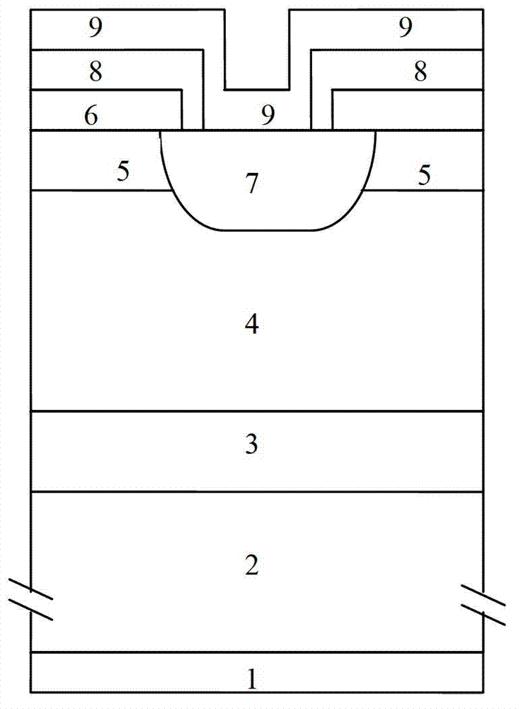
[0024] see figure 1 , the GaAsP / GaP PIN PD embodiment is provided with epitaxial wafers, and the epitaxial wafers are sequentially provided with n-type highly doped gallium phosphide single crystals from bottom to top Substrate 2, non-doped gallium phosphide buffer layer 3, non-doped GaAs 0.15 P 0.85 The light absorbing layer 4 and the non-doped gallium phosphide cap layer 5 are provided with an n-type ohmic contact electrode 1 at the bottom of the n-type highly doped gallium phosphide single crystal substrate 2 of the epitaxial wafer; A silicon nitride mask 6, a p-type highly doped diffusion layer 7 formed by zinc diffusion, a p-type ohmic contact electrode 8 and a silicon nitride antireflection film 9 are sequentially grown on the gallium phosphide cap layer 5.

[0025] The manufacturing method of the gallium arsenide phosphide / gallium phosphide yellow light narrow-band detector comprises the following steps:

[0026] 1) Insert the epitaxial wafer (see figure 1 ) cleanin...


PUM


Abstract

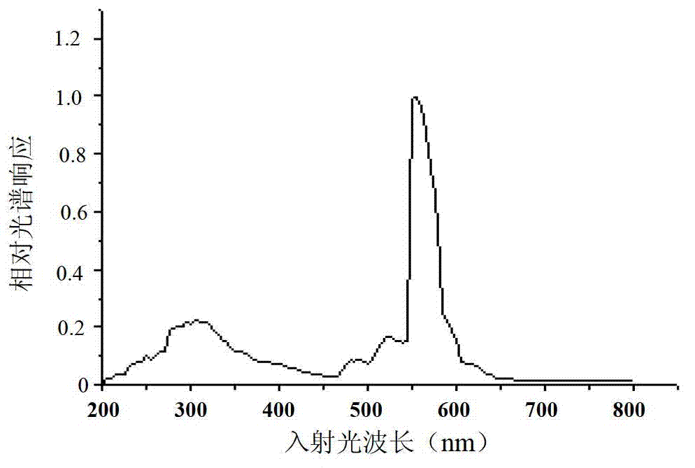
The invention discloses a gallium, arsenic and phosphorus / gallium phosphide yellow light narrow-band detector and a manufacturing method of the gallium, arsenic and phosphorus / gallium phosphide yellow light narrow-band detector, and relates to a detector. The invention provides the gallium, arsenic and phosphorus / gallium phosphide yellow light narrow-band detector for detection of an infrared up-conversion material and the manufacturing method thereof. The detector is provided with an epitaxial wafer which is sequentially provided with an n-type high doping gallium phosphide monocrystal substrate, a non-doping gallium phosphide buffer layer, a non-doping GaAs0.15P0.85 light absorbing layer and a non-doping gallium phosphide cap layer from bottom to top. An n-type ohmic contact electrode is arranged at the bottom of the n-type high doping gallium phosphide monocrystal substrate. A silicon nitride mask, a p-type high-doping diffusing layer formed through zinc diffusion, a p-type ohmic contact electrode and a silicon nitride antireflection film grow sequentially on the non-doping gallium phosphide cap layer of the epitaxial wafer. The gallium, arsenic and phosphorus / gallium phosphide yellow light narrow-band detector has the advantages of easiness in preparation, low cost, nearly no response to infrared light and the like, and can be used to detect the infrared up-conversion material such as bill and the like, so that the bill detecting capacity of a bill detector is improved.

Description

technical field [0001] The invention relates to a detector, in particular to a gallium arsenide phosphide / gallium phosphide (GaAsP / GaP) yellow light narrow-band detector and a manufacturing method thereof. Background technique [0002] Infrared up-conversion materials are optical functional materials that use invisible infrared light to excite visible light (usually yellow light). Anti-counterfeiting technology. High-efficiency infrared up-conversion materials are relatively expensive to use. Therefore, when mixing inks, it is required to reduce the content of conversion materials as much as possible. In this way, the intensity of visible light converted by up-conversion inks will be very weak. In addition, in practical applications, the optical power of infrared lasers is much greater than that of visible light emitted by up-conversion materials. Therefore, infrared laser is also a powerful "interference source" for photosensitive detection devices. Therefore, higher req...

Claims


Application Information

Patent Timeline
Patent Type & Authority Applications(China)
IPC IPC(8): H01L31/0304H01L31/105H01L31/18
CPCY02P70/50
Inventor 肖雪芳陈朝
Owner XIAMEN UNIV OF TECH
Learn More