Polycrystalline silicon ingot, manufacturing method thereof and solar cell
A technology of polycrystalline silicon ingots and manufacturing methods, which is applied to the growth of polycrystalline materials, chemical instruments and methods, circuits, etc., and can solve the problems of many grain boundaries and dislocations, small grains, and low attenuation coefficients of polycrystalline silicon solar cells
- Summary
- Abstract
- Description
- Claims
- Application Information
AI Technical Summary
Problems solved by technology
Method used
Image
Examples
Embodiment 1
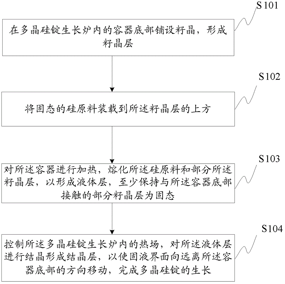
[0111] Based on the above research, an embodiment of the present invention provides a method for manufacturing a polycrystalline silicon ingot. The flowchart of the method is as follows: figure 1 As shown, including the following steps:
[0112] Step S101: laying seed crystals on the bottom of the container in the polysilicon ingot growth furnace to form a seed crystal layer;
[0113] Wherein, the seed layer may be a whole large single crystal seed crystal having the same size and shape as the bottom of the container, or it may be formed by splicing a plurality of small single crystal seed crystals. In addition, the seed crystal is a single crystal silicon with a fixed crystallographic orientation, and the seed layer includes at least one single crystal silicon layer with a crystallographic orientation. Preferably, the seed crystal in this embodiment is (100), ( 110) or (111) oriented single crystal silicon.
[0114] Specifically, the seed layer in this embodiment includes at least ...
Embodiment 2
[0136] In the normal ingot casting process, after the crystal growth is completed, the crystal needs to be cooled to a certain temperature, the polycrystalline silicon ingot is removed from the ingot furnace, and then the polycrystalline silicon ingot is further processed.
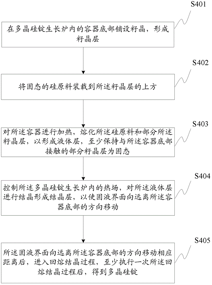
[0137] As described in step 104 in the first embodiment, the crystallization rate of molten silicon will affect the quality of the final product. The growth rate can be slowed to reduce the hard spots and impurity-rich layers in the product. The growth rate of the crystal is relatively difficult to control. To avoid the above-mentioned defects, this embodiment is based on the first embodiment. figure 1 The process of completing the crystal growth in step S104 is further defined, and the specific process of polycrystalline silicon ingot formation is described in detail.
[0138] See figure 2 In this embodiment, the thermal field in the polycrystalline silicon ingot growth furnace is controlled, and the liquid la...
Embodiment 3
[0148] The flow chart of the manufacturing method of the polycrystalline silicon ingot disclosed in this embodiment is shown in 4. The difference from the above two embodiments is that the selection of the seed crystal, the method of forming the seed layer, and the loading of silicon raw materials are used in this embodiment. Process specificity, Figure 4 Only the method in Embodiment 2 is used as an example for description. Of course, the method in this embodiment can also be applied to the method in Embodiment 1. The method in this embodiment includes the following steps:
[0149] Step S201: at the bottom of the container in the polysilicon ingot growth furnace, splicing and tiling seed crystals with the same crystallographic orientation to form the seed layer, the seed layer being substantially parallel to the bottom of the container;
[0150] In this embodiment, it is preferable to use (100)-oriented monocrystalline silicon to form the seed layer. Preferably, the area of the ...
PUM
| Property | Measurement | Unit |
|---|---|---|
| thickness | aaaaa | aaaaa |
| thickness | aaaaa | aaaaa |
| thickness | aaaaa | aaaaa |
Abstract
Description
Claims
Application Information
 - R&D
- Intellectual Property
- Life Sciences
- Materials
- Tech Scout
- Unparalleled Data Quality
- Higher Quality Content
- 60% Fewer Hallucinations
Browse by: Latest US Patents, China's latest patents, Technical Efficacy Thesaurus, Application Domain, Technology Topic, Popular Technical Reports.
© 2025 PatSnap. All rights reserved.Legal|Privacy policy|Modern Slavery Act Transparency Statement|Sitemap|About US| Contact US: help@patsnap.com


