NOR memory cell based on resistance-changeable gate dielectric, its array and its operation method

A technology of memory cells and gate dielectrics, applied in the field of memory, can solve problems such as thinning of floating gates, and achieve the effects of low power consumption, simple process and high performance

Inactive Publication Date: 2012-11-21
FUDAN UNIV
View PDF4 Cites 5 Cited by
  • Summary
  • Abstract
  • Description
  • Claims
  • Application Information

AI Technical Summary

Problems solved by technology

[0007] 3. NOR-type flash memory Flash is a charge-storage device. With the shrinking of the feature size in the semiconductor process, the floating gate for storing charges cannot be thinned without limit, and there is a physical limit

Method used


Image

  • NOR memory cell based on resistance-changeable gate dielectric, its array and its operation method
  • NOR memory cell based on resistance-changeable gate dielectric, its array and its operation method
  • NOR memory cell based on resistance-changeable gate dielectric, its array and its operation method

Examples


Embodiment Construction

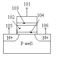
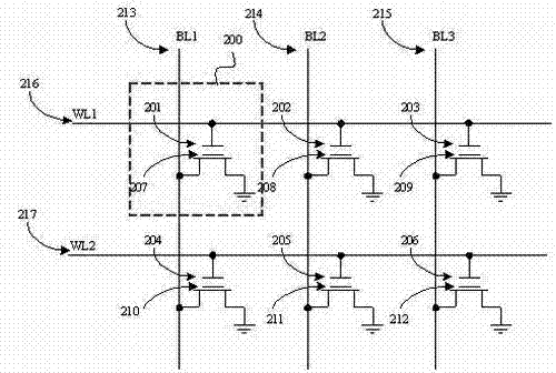
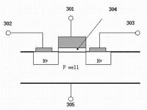
[0024] According to an embodiment of the present invention, the NOR memory based on the resistive gate dielectric includes: a transistor, including a source, a drain, and a control gate; a storage node, that is, the gate dielectric of the transistor control gate, located between the transistor control gate and Among the silicon substrates, the storage resistance changes; the word line is connected to the control gate of the transistor; the bit line is connected to the drain of the transistor; the source line is connected to the source of the transistor. Reference attached image 3 , is a NOR memory cell based on a resistive gate dielectric according to an embodiment of the present invention. Wherein, 301 is a word line (Wordline), 302 and 303 are respectively a source line (Sourceline) and a bit line (Bitline), and the gate 304 is made of a material with resistive properties, such as HfOx. Among them, the gate 304 has three different states of insulation, high resistance and ...


PUM


Abstract

An NOR memory based on a resistance-changeable gate dielectric comprises: a transistor comprising a source electrode, a drain electrode and a control gate electrode; a memory node which is a gate dielectric of the control gate electrode of the transistor, is positioned between the control gate electrode of the transistor and a silicon substrate and stores the resistance change; a word line connected to the control gate electrode of the transistor; a bit line connected to the drain electrode of the transistor; and a source line connected to the source electrode of the transistor. The gate electrode uses a resistance-changeable characteristic material having three different states of insulation, high resistance and low resistance, there is reversible switching between the high resistance and the low resistance, a constant voltage is applied among the word line, the source line and the bit line during reading, and "0" and "1" can be determined according to different currents. The invention also provides an array and an operation method of the NOR memory cell based on the resistance-changeable gate dielectric.

Description

technical field [0001] The invention relates to the field of memory technology, in particular to a device for non-volatile storage, a NOR array structure, and an operation method thereof. Background technique [0002] Memory occupies an important position in the semiconductor market. Due to the continuous popularization of portable electronic devices, the share of non-volatile memory in the entire memory market is also increasing, of which more than 90% of the share is occupied by FLASH. However, due to the requirement of storing charges, the floating gate of FLASH cannot be thinned without limit with the development of technology generation. It is reported that the limit of FLASH technology is around 32nm, which forces people to look for the next generation of non-volatile memory with better performance. Recently, resistive switching memory (resistive switching memory) has attracted high attention because of its high density, low cost, and the characteristics of breaking th...

Claims


Application Information

Patent Timeline
Patent Type & Authority Applications(China)
IPC IPC(8): G11C16/02G11C16/08
Inventor 林殷茵李慧
Owner FUDAN UNIV
Why Eureka
Try Eureka