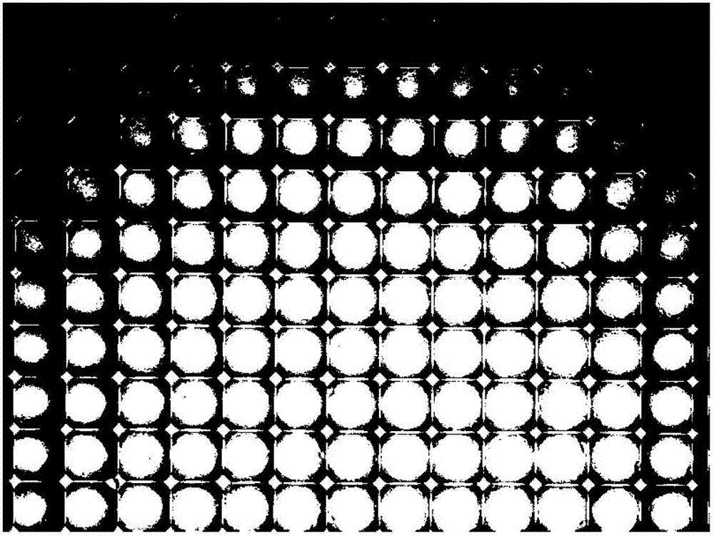
Method for enhancing chemical etching through femtosecond laser to manufacture large-scale micro-lens array
A technology of microlens array and femtosecond laser, applied in laser welding equipment, optics, lenses, etc., can solve the problems of low production efficiency, uncontrollable shape, high cost, etc., and achieve the effect of efficient processing technology
- Summary
- Abstract
- Description
- Claims
- Application Information
AI Technical Summary
Problems solved by technology
Method used
Image
Examples
Embodiment 1
[0026] A method for preparing a large-scale microlens array by using femtosecond laser enhanced chemical etching, comprising the following steps:
[0027] Step 1. Select the hard material used as the femtosecond laser target, put it into three solutions of acetone, ethanol, and deionized water in order to clean thoroughly, then place the target on the femtosecond laser micro-nano processing device, and select the pulse An ultrashort pulse laser with a width of 30fs and a wavelength of 800nm is focused on the surface of a hard material through an objective lens with a numerical aperture of 0.5;
[0028] Step 2. According to the shape of the rectangular microlens array to be processed, control the speed at which the precision machining platform moves the target. The femtosecond laser acts on the surface of the target for 500 pulses. Due to the special processing characteristics of the femtosecond laser, on the target A photodestructive zone is generated centered on the focus o...
Embodiment 2
[0034] A method for preparing a large-scale microlens array by using femtosecond laser enhanced chemical etching, comprising the following steps:
[0035] Step 1. Select the hard material used as the femtosecond laser target, put it into three solutions of acetone, ethanol, and deionized water in order to clean thoroughly, then place the target on the femtosecond laser micro-nano processing device, and select the pulse An ultrashort pulse laser with a width of 30fs and a wavelength of 800nm is focused on the surface of a hard material through an objective lens with a numerical aperture of 0.5;
[0036] Step 2. According to the shape of the rectangular microlens array to be processed, control the speed at which the precision machining platform moves the target. The femtosecond laser acts on the surface of the target for 500 pulses. Due to the special processing characteristics of the femtosecond laser, on the target A photodestructive zone is generated centered on the focus o...
Embodiment 3
[0042] A method for preparing a large-scale microlens array by using femtosecond laser enhanced chemical etching, comprising the following steps:
[0043] Step 1. Select the hard material used as the femtosecond laser target, put it into three solutions of acetone, ethanol, and deionized water in order to clean thoroughly, then place the target on the femtosecond laser micro-nano processing device, and select the pulse An ultrashort pulse laser with a width of 30fs and a wavelength of 800nm is focused on the surface of a hard material through an objective lens with a numerical aperture of 0.5;
[0044]Step 2. According to the shape of the rectangular microlens array to be processed, control the speed at which the precision machining platform moves the target. The femtosecond laser acts on the surface of the target for 1000 pulses. Due to the special processing characteristics of the femtosecond laser, on the target A photo-destructive zone is generated centered on the focus ...
PUM
| Property | Measurement | Unit |
|---|---|---|
| Diameter | aaaaa | aaaaa |
Abstract
Description
Claims
Application Information
 - Generate Ideas
- Intellectual Property
- Life Sciences
- Materials
- Tech Scout
- Unparalleled Data Quality
- Higher Quality Content
- 60% Fewer Hallucinations
Browse by: Latest US Patents, China's latest patents, Technical Efficacy Thesaurus, Application Domain, Technology Topic, Popular Technical Reports.
© 2025 PatSnap. All rights reserved.Legal|Privacy policy|Modern Slavery Act Transparency Statement|Sitemap|About US| Contact US: help@patsnap.com


