Polycrystalline silicon ingot, preparation method of polycrystalline silicon ingot, polycrystalline silicon slice and crucible for polycrystalline silicon ingot casting
A technology for polycrystalline silicon ingots and polycrystalline silicon wafers, which is applied to the growth of polycrystalline materials, chemical instruments and methods, and crystal growth. It can solve the problems that other crystal grains are not easy to grow, easy to squeeze each other, and generate stress. It is suitable for large-scale The effect of production, easy operation, and high conversion efficiency
- Summary
- Abstract
- Description
- Claims
- Application Information
AI Technical Summary
Problems solved by technology
Method used
Image
Examples
Embodiment 1
[0043] The preparation method of polycrystalline silicon ingot comprises the following steps:
[0044] (1) A nucleation source is arranged at the bottom of the crucible to form a nucleation source layer;
[0045] Among them, the nucleation source is set at the bottom of the crucible: use a mixture of silicon powder and silicon nitride powder totaling 300g, wherein the mass ratio of silicon powder and silicon nitride powder is 6:4, with 500ml of alcohol, brush on the bottom of the crucible Coated and baked in a crucible oven at 800 degrees for 2 hours. The particle size of the silicon powder is 10um, and the particle size of the silicon nitride powder is 0.5-50um.
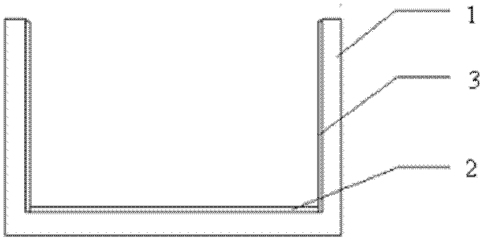
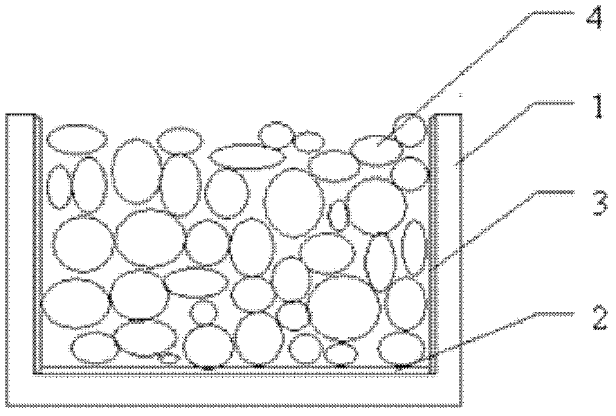
[0046] figure 1 It is a schematic diagram of the crucible for polycrystalline silicon ingot prepared in Example 1 of the present invention. Wherein, 1 is the crucible body, 2 is the nucleation source layer, and 3 is the silicon nitride layer coated on the side wall of the crucible.
[0047] (2) setting molten si...
Embodiment 2
[0056] The preparation method of polycrystalline silicon ingot comprises the following steps:
[0057] (1) A nucleation source is arranged at the bottom of the crucible to form a nucleation source layer;
[0058] Among them, the nucleation source is set at the bottom of the crucible: a total of 200g of a mixture of silicon carbide and silicon nitride powder is used, wherein the mass ratio of silicon carbide and silicon nitride powder is 8:2, with 500ml of water, using a compressed air spray gun, spraying On the bottom of the crucible, bake in a 1000 degree crucible oven for 2 hours. The particle size of silicon carbide and silicon nitride powder is 20um.
[0059] (2) setting molten silicon material on the nucleation source layer;
[0060] Among them, setting the molten silicon material on the nucleation source layer is as follows: 450-800 kg of solid silicon material is loaded above the nucleation source layer, and the crucible is heated to 1560 ° C to melt the solid silicon...
Embodiment 3
[0066] The preparation method of polycrystalline silicon ingot comprises the following steps:
[0067] (1) A nucleation source is arranged at the bottom of the crucible to form a nucleation source layer;
[0068] Among them, the nucleation source is set at the bottom of the crucible: use a mixture of carbon powder and silicon nitride powder totaling 300g, wherein the mass ratio of silicon carbide and silicon nitride powder is 6:4, with 500ml of alcohol, brush on the bottom of the crucible Coated and baked in a crucible oven at 800 degrees for 2 hours. The particle size of the carbon powder is 20um, and the particle size of the silicon nitride powder is 5um.
[0069] (2) setting molten silicon material on the nucleation source layer;
[0070] Among them, setting the silicon material in molten state on the nucleation source layer is: heating 450-800 kg of solid silicon material in another crucible to 1560 ° C to obtain molten silicon material, and casting the molten silicon ma...
PUM
| Property | Measurement | Unit |
|---|---|---|
| particle diameter | aaaaa | aaaaa |
| particle diameter | aaaaa | aaaaa |
| particle diameter | aaaaa | aaaaa |
Abstract
Description
Claims
Application Information
 - Generate Ideas
- Intellectual Property
- Life Sciences
- Materials
- Tech Scout
- Unparalleled Data Quality
- Higher Quality Content
- 60% Fewer Hallucinations
Browse by: Latest US Patents, China's latest patents, Technical Efficacy Thesaurus, Application Domain, Technology Topic, Popular Technical Reports.
© 2025 PatSnap. All rights reserved.Legal|Privacy policy|Modern Slavery Act Transparency Statement|Sitemap|About US| Contact US: help@patsnap.com


