GaN-based LED with dual reflecting layers

A light-emitting diode, gallium nitride-based technology, applied in semiconductor devices, electrical components, circuits, etc., can solve the problems that light cannot or is difficult to emit from the side or above, affect the luminous efficiency of the chip, and cannot take out light, etc. The effect of light extraction efficiency, improvement of luminous distribution uniformity, and reduction of current accumulation

Active Publication Date: 2012-10-03
ANHUI SANAN OPTOELECTRONICS CO LTD
View PDF3 Cites 9 Cited by
  • Summary
  • Abstract
  • Description
  • Claims
  • Application Information

AI Technical Summary

Problems solved by technology

Since the metal reflective layer 104 (usually Al or Ag material) has a reflective effect on light, the light emitted by the light-emitting layer is emitted and emitted from the side, as shown by light 1a; however, some light cannot or is difficult to pass through from the side Or above, as shown by light 1b, resulting in light loss, unable to effectively extract the light emitted by the light-emitting layer, which affects the luminous efficiency of the chip

Method used


Image

  • GaN-based LED with dual reflecting layers
  • GaN-based LED with dual reflecting layers
  • GaN-based LED with dual reflecting layers

Examples


Embodiment 1

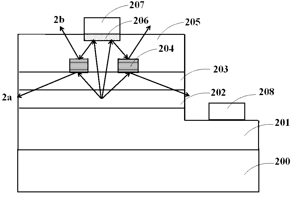
[0061] Such as figure 2 and image 3 A gallium nitride-based high-brightness light-emitting diode with double reflective layers is shown, including: a sapphire substrate 200, an N-type layer 201, a light-emitting region 202, a P-type layer 203, an annular distributed Bragg reflective layer 204, A current spreading layer 205 , a metal reflective layer 206 , a P electrode 207 and an N electrode 208 .

[0062] Specifically, the lowest layer in the above light emitting diode structure is the sapphire substrate 200; the N-type layer 201 is formed on the sapphire substrate 200; the light-emitting region 202 is formed on the N-type layer 201; the P-type layer 203 is formed on the light-emitting On the region 202; the annular distributed Bragg reflection layer 204 is formed on the P-type layer 203; the ITO current spreading layer 205 is formed on the surface of the annular distributed Bragg reflection layer 204 and the P-type layer 203; Al metal reflector Layer 206, formed on the s...

Embodiment 2

[0074] Compared with Embodiment 1, this embodiment discloses a gallium nitride-based high-brightness light-emitting diode with a vertical structure and double reflective layers. In this embodiment, Si is used as the substrate 200, and the N electrode 208 is formed on the back of the substrate, forming a vertical LED device structure.

Embodiment 3

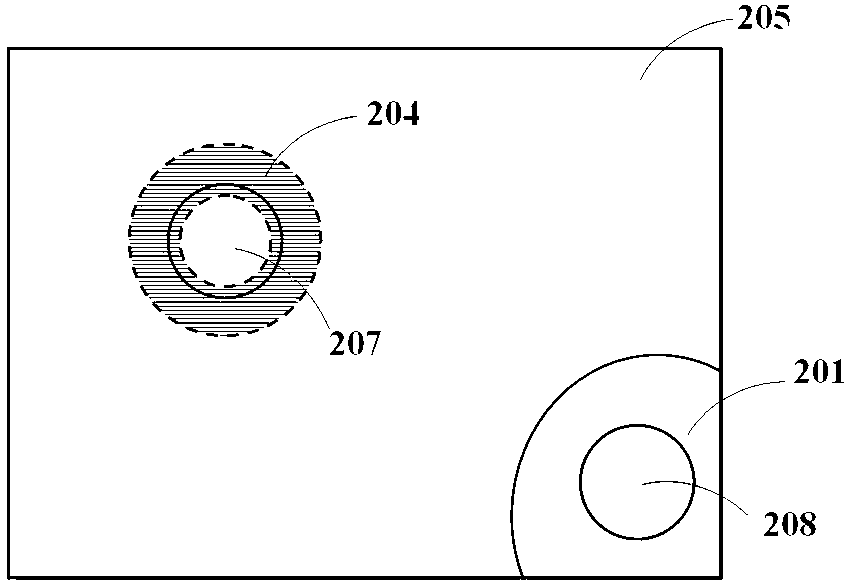
[0076] Compared with Embodiment 1, the electrode structure of the gallium nitride-based LED device disclosed in this embodiment further includes an extended electrode 209 with a width of 10 microns, and a metal reflective layer and a ring-shaped reflective layer can be arranged directly under the extended electrode 209, Further improve the light extraction efficiency. The metal reflective layer can be as large as the extended electrode, and the ring-shaped reflective layer is composed of a ring-shaped structure 204 below the P electrode 207 and a strip-shaped ring structure 210 below the extended electrode 209 . The difference between the annular structure 204 and Embodiment 1 is that the inner diameter of the annular distributed Bragg reflection layer 204 is 80 microns, which is equivalent to the diameter of the P electrode 207, and the inner diameter of the elongated annular structure 210 is 10 microns. , with an outer ring diameter of 20 μm.


PUM


Abstract

The invention relates to a GaN-based LED with dual reflecting layers. The GaN-based LED comprises a substrate, an epitaxial layer, a current extension layer and a P electrode, wherein the epitaxial layer is formed on the substrate and comprises a P-type layer, a light-emitting region and an N-type layer; the current extension layer is formed on the P-type layer; and the P electrode is formed on the current extension layer. The GaN-based LED is characterized in that a reflecting structure is formed between the P electrode and the epitaxial layer and is composed of an annular reflecting layer and a metal reflecting layer, wherein the geometric center of the reflecting structure corresponds to the P electrode in the vertical direction, and the annular reflecting layer is formed between the current extension layer and the P-type layer; the metal reflecting layer is formed between the current extension layer and the P electrode; and a preset distance is reserved between the annular reflecting layer and the metal reflecting layer. According to the invention, the annular reflecting layer and the metal reflecting layer are additionally arranged between the epitaxial layer and the P electrode of the LED, so that light emitted from the light-emitting layer can be effectively taken out, the light absorption phenomenon of the P electrode is reduced, and therefore the light-emitting efficiency is increased.

Description

technical field [0001] The invention relates to a gallium nitride-based light-emitting diode, in particular to a gallium nitride-based high-brightness light-emitting diode with double reflection layers. Background technique [0002] At present, blue-green LEDs use GaN-based III-V compound semiconductor materials; due to the small hole concentration of the P-GaN layer of GaN-based LED epitaxial wafers, and the thickness of the P-type layer is very thin, most of the luminescence comes from The P-type layer leaks out, and the P-type layer inevitably absorbs light, resulting in low external quantum efficiency of the LED chip, which greatly reduces the luminous efficiency of the LED. Although the transmittance can be improved by using the ITO layer as the current spreading layer, the voltage of the LED is higher, and the lifetime is also affected. In addition, under the applied voltage, due to the uneven current diffusion, the current density in some areas is very high, which af...

Claims


Application Information

Patent Timeline
Patent Type & Authority Applications(China)
IPC IPC(8): H01L33/10
CPCH01L33/10H01L33/405H01L2924/0002H01L33/14H01L33/32H01L2924/00H01L25/13H01L33/60
Inventor 郑建森林素慧彭康伟洪灵愿何安和
Owner ANHUI SANAN OPTOELECTRONICS CO LTD
Why Eureka
Try Eureka