Method for producing nitride crystals, and production vessel and members
A manufacturing method and nitride technology, applied in the field of ammonothermal method, can solve problems such as hindering crystal growth and lowering productivity, and achieve the effect of improving production efficiency and high quality
- Summary
- Abstract
- Description
- Claims
- Application Information
AI Technical Summary
Problems solved by technology
Method used
Image
Examples
Embodiment 1)
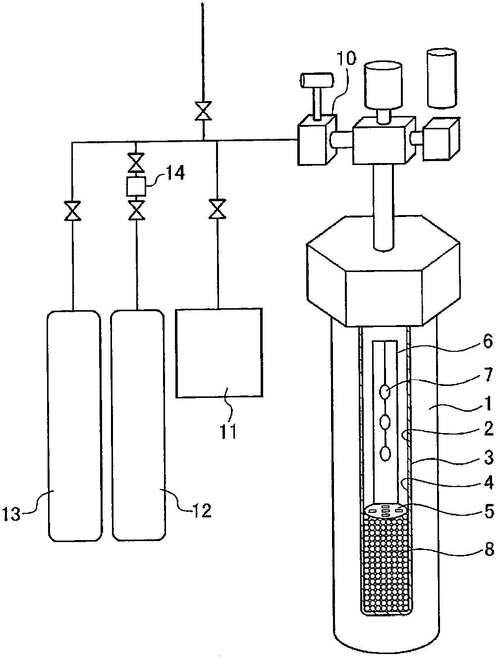
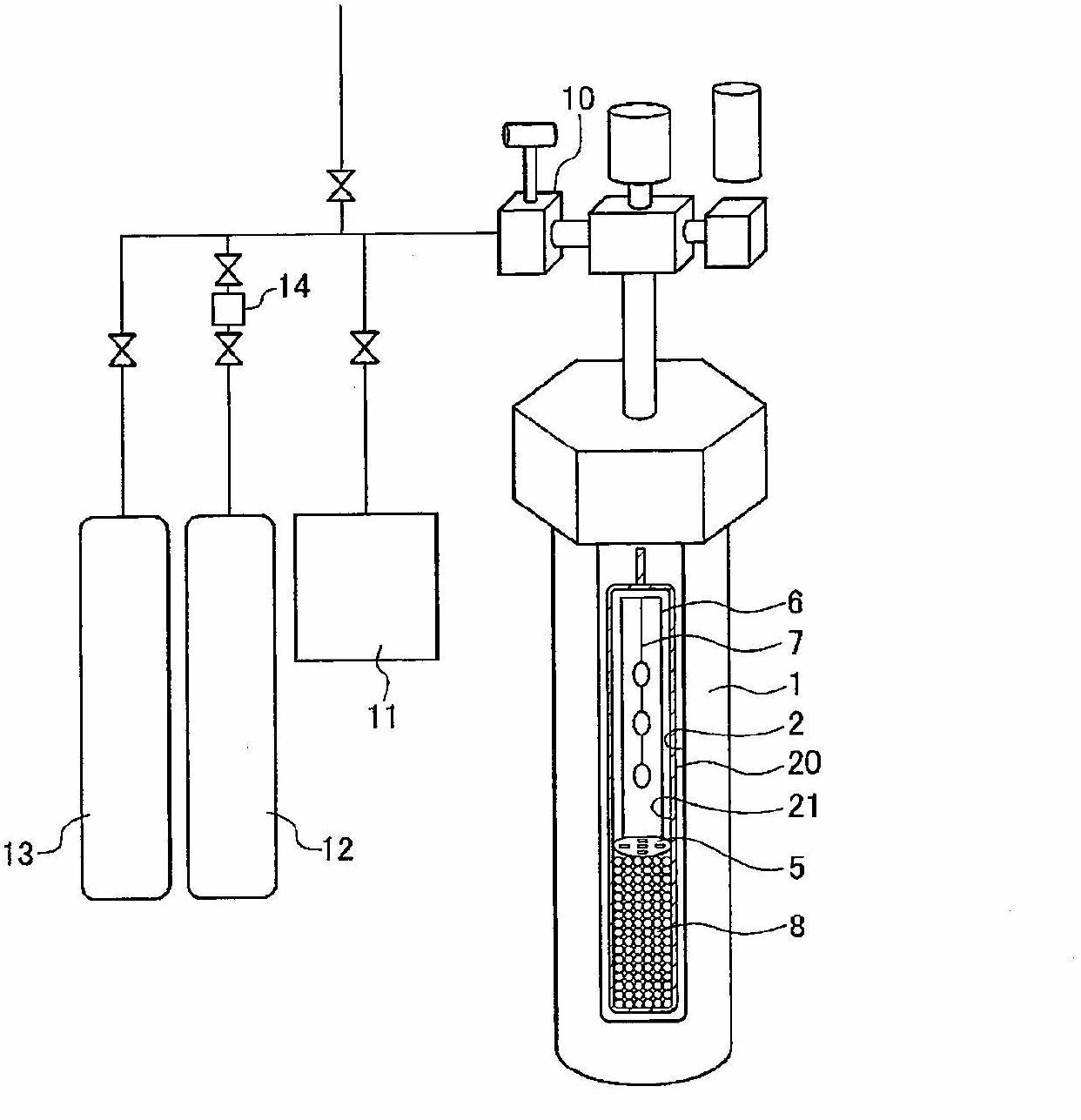
[0160] In this example, use figure 1 In the shown reaction device, the seed crystal and the test piece are suspended, and the experiment of heating the raw material is carried out.
[0161] An autoclave 1 made of Inconel 625 with a platinum-lined inner size of 15 mm in diameter and 154 mm in length (inner volume of about 27 cm 3 ),conduct experiment. The inner surface 2 of the autoclave 1 is thoroughly cleaned and dried. Similarly, platinum wires, platinum growth frames 6 , platinum baffles 5 , and platinum mesh raw material baskets used to support the test pieces were washed and dried.
[0162] Polycrystalline GaN particles were used as raw material 8 for nitride crystal growth. The polycrystalline GaN particles were washed with hydrofluoric acid at a concentration of about 50% by weight for the purpose of removing deposits, rinsed sufficiently with pure water, dried, and weighed 12.98 g into a raw material basket made of platinum mesh.
[0163] Weigh 0.74 g of fully drie...
Embodiment 2)
[0194] In Example 2, a bulk Ta-2.5% by weight W alloy was used as a test piece. The experiment was carried out under the same conditions as in Example 1 except that the point where the seed crystal was not attached was changed.
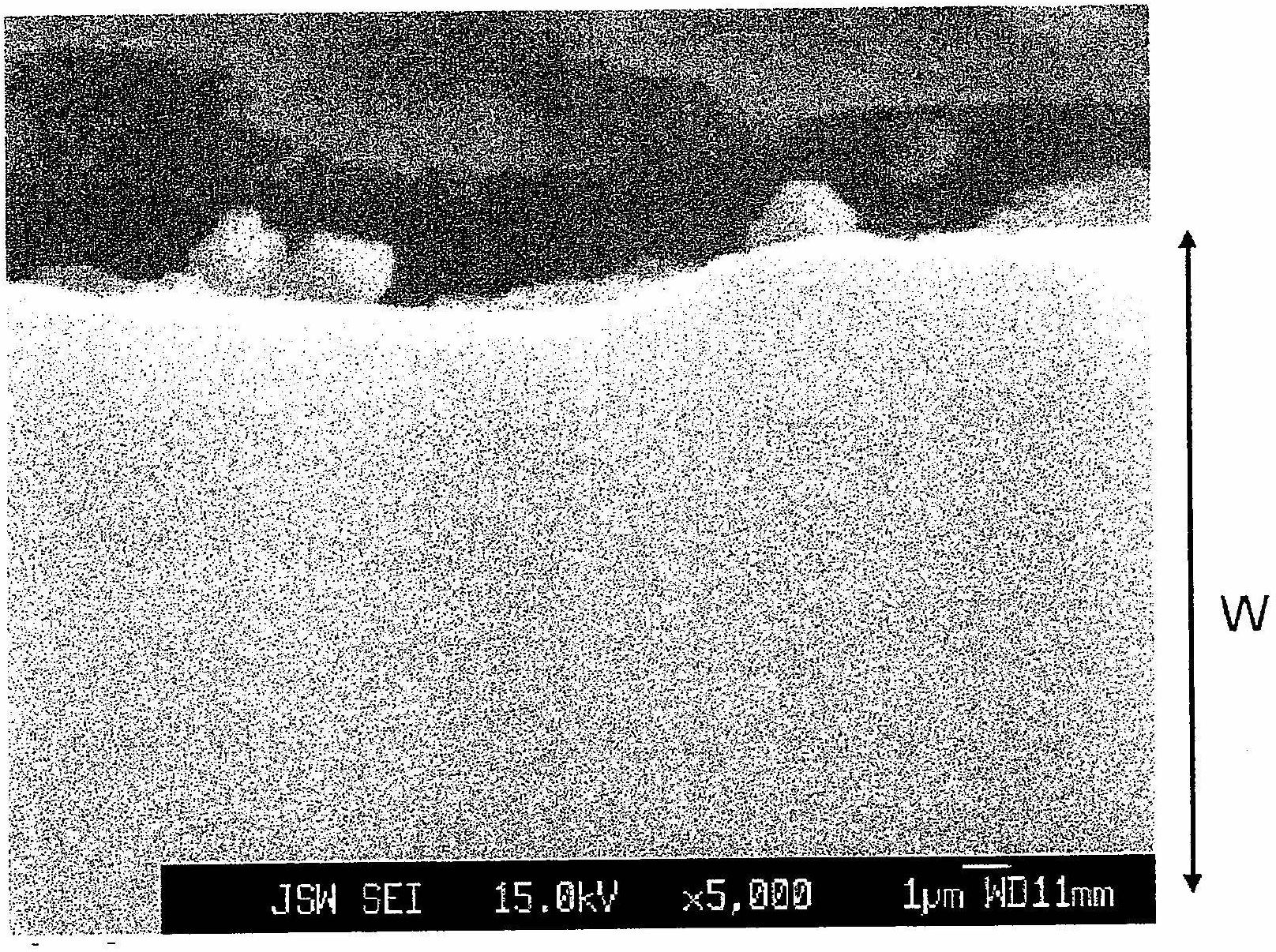
[0195] As a result of observing the appearance of the test piece after implementation of Example 2, there was almost no change from before implementation, and no deposits were observed. In the measurement by EPMA, the formation of GaN was not found on the surface. As a result of observing the unevenness of the test piece by a cross-sectional SEM, almost no unevenness was found.
[0196] The surface roughness of the same test piece as that of Example 2 was measured before the suspension test, and the surface roughness (Ra) was 0.463 μm. As a result of observing the cross section by EPMA, no nitride layer or other deteriorated layer was found on the surface of the test piece, and no corrosion was confirmed.
Embodiment 3)
[0198] In Example 3, plate-shaped tantalum was used as a test piece. The experiment was carried out under the same conditions as in Example 1 except that the point where the seed crystal was not attached was changed.
[0199] As a result of observing the appearance of the test piece after implementation of Example 3, there was almost no change from before implementation, and no deposits were observed. In the measurement by EPMA, the formation of GaN was not found on the surface. As a result of observation of irregularities of the test piece by cross-sectional SEM, it was confirmed that the cross section was extremely flat.
[0200] The surface roughness of the same test piece as that of Example 3 was measured before the suspension test, and the surface roughness (Ra) was 0.079 μm. As a result of observing the cross section by EPMA, no nitride layer or other deteriorated layer was found on the surface of the test piece, and no corrosion was confirmed.
PUM
| Property | Measurement | Unit |
|---|---|---|
| surface roughness | aaaaa | aaaaa |
| thickness | aaaaa | aaaaa |
| thickness | aaaaa | aaaaa |
Abstract
Description
Claims
Application Information
 - R&D
- Intellectual Property
- Life Sciences
- Materials
- Tech Scout
- Unparalleled Data Quality
- Higher Quality Content
- 60% Fewer Hallucinations
Browse by: Latest US Patents, China's latest patents, Technical Efficacy Thesaurus, Application Domain, Technology Topic, Popular Technical Reports.
© 2025 PatSnap. All rights reserved.Legal|Privacy policy|Modern Slavery Act Transparency Statement|Sitemap|About US| Contact US: help@patsnap.com


