Image sensor

A technology of image sensor and photosensitive device, which is applied in the direction of image communication, TV, color TV parts, etc. It can solve the problems of crosstalk, limited light-gathering effect of microlens, low refractive index, etc., so as to reduce crosstalk and improve effective photosensitivity efficiency Effect

Active Publication Date: 2012-09-26
SHANGHAI ADVANCED RES INST CHINESE ACADEMY OF SCI
View PDF4 Cites 1 Cited by
  • Summary
  • Abstract
  • Description
  • Claims
  • Application Information

AI Technical Summary

Problems solved by technology

[0006] However, in actual work, due to the extremely small size of the pixel unit compared to the external environment to be detected, the light-gathering effect of the microlens is limited. After a large amount of light enters the interlayer dielectric layer, it will not only enter the photosensitive area of ​​the corresponding pixel , will also enter adjacent pixels, causing crosstalk and reducing the effective photosensitive efficiency of the photosensitive area
[0007] In the prior art, it has been proposed that an air hole is formed by etching around the dielectric layer above the photosensitive area, thereby forming a waveguide-like optical path above the photosensitive area, limiting most of the incident light to be transmitted in this path, but This method has limited restrictions on light, especially the dielectric layer above the photosensitive area is usually a low dielectric constant material, and the refractive index is usually low (generally about 1.5); in addition, it has also been proposed that the dielectric layer above the photosensitive area Around, a continuous metal layer is used as a reflective layer to prevent the impact of incident light on adjacent pixels, but metal has a certain absorption effect on electromagnetic waves. With the further shrinking of the size of CMOS image sensors, for certain limit wavelengths of light, It can be regarded as an electromagnetic wave approximately, but the absorption effect of metal cannot be ignored

Method used


Image

  • Image sensor
  • Image sensor
  • Image sensor

Examples


Embodiment Construction

[0020] In the following description, many technical details are proposed in order to enable readers to better understand the application. However, those skilled in the art can understand that without these technical details and various changes and modifications based on the following implementation modes, the technical solution claimed in each claim of the present application can be realized.

[0021] In order to make the purpose, technical solution and advantages of the present invention clearer, the following will further describe the implementation of the present invention in detail in conjunction with the accompanying drawings.

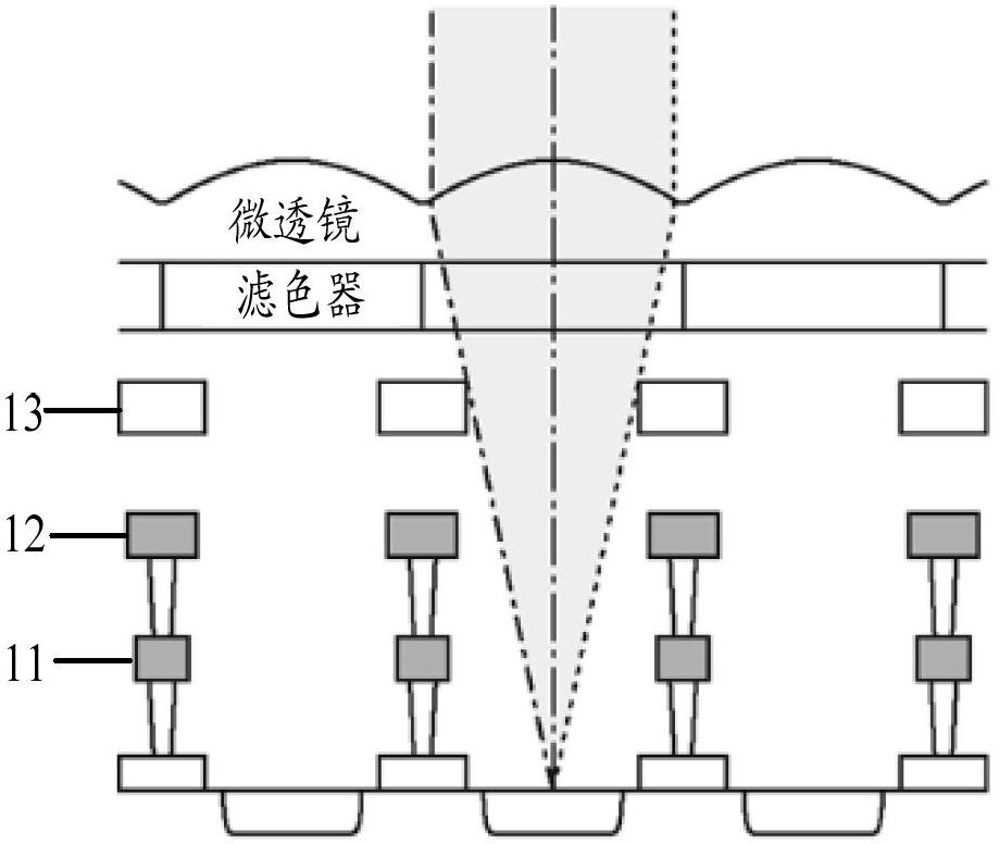
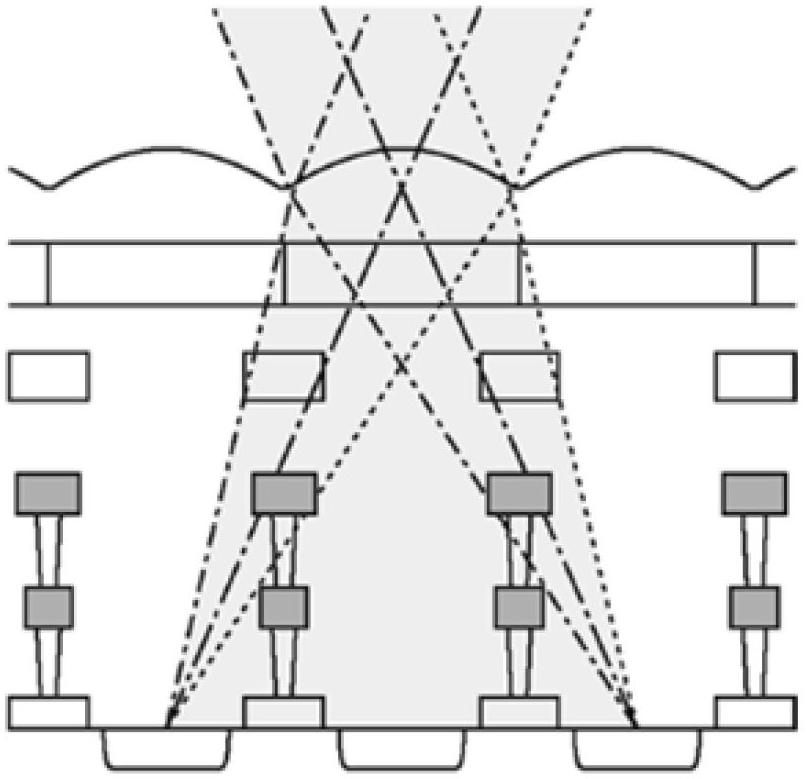
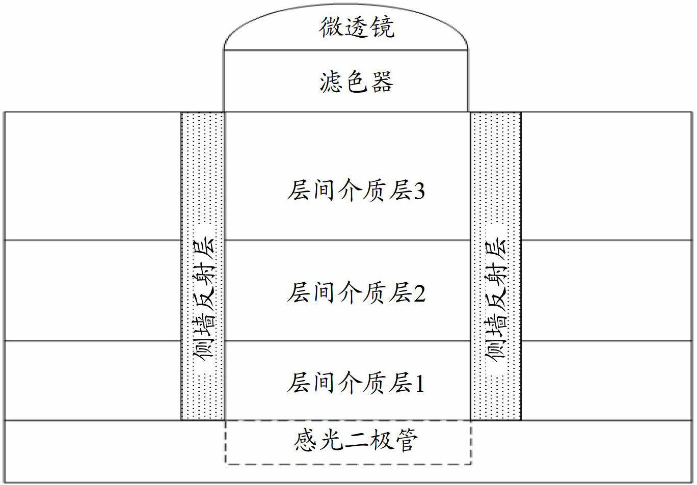
[0022] A first embodiment of the present invention relates to an image sensor. image 3 is a schematic diagram of the image sensor structure.

[0023] Specifically, as image 3 As shown, the image sensor includes a plurality of pixel areas, each pixel area includes a photosensitive device, the surface of each photosensitive device is covered wit...


PUM


Abstract

The invention relates to the technical field of semiconductors and discloses an image sensor. A laminated layer formed by a first medium layer, a second medium layer and a third medium layer is taken as a side wall reflection layer around a medium layer above the surface of a photosensitive area, so that a light path is constructed; light is limited in a corresponding pixel photosensitive area to be prevented from being emitted into an adjacent pixel photosensitive area; and therefore, the cross-interference can be reduced, and the effective photosensitive efficiency of the photosensitive area can be improved. The image sensor has the beneficial effects that the incident light is limited on the basis of a refractive index difference between the first medium layer and the interlamination medium layer, and the second medium layer, namely the metal layer, only reflects the light transmitting through the first medium layer, so that the absorption effect of metal on the light is relieved to a certain extent; and furthermore, the laminated structure ensures a polishing effect during a subsequent chemical-mechanical polishing process, and the metal can be prevented from falling off and stripping.

Description

technical field [0001] The invention relates to the technical field of semiconductors, in particular to an image sensor with a light path. Background technique [0002] As we all know, an image sensor is a semiconductor device that converts an optical image into an electrical signal. Image sensors can be roughly classified into charge-coupled device (Charge-Coupled Device, “CCD” for short) and complementary metal oxide semiconductor (Complementary Metal Oxide Semiconductor, “CMOS” for short) image sensors. [0003] According to its readout method, the existing CMOS image sensors can be roughly divided into passive pixel sensor (Passive Pixel Sensor, referred to as "PPS"), active pixel sensor (Active Pixel Sensor, referred to as "APS") and digital pixel sensor There are three types of sensors (Digital Pixel Sensor, referred to as "DPS"). [0004] figure 1 and figure 2 are the photosensitive conditions in the image sensor structure under ideal conditions and actual condit...

Claims


Application Information

Patent Timeline
IPC IPC(8): H01L27/146H04N5/374
Inventor 方娜田犁陈杰汪辉苗田乐
Owner SHANGHAI ADVANCED RES INST CHINESE ACADEMY OF SCI
Why Eureka
Try Eureka