Small-size CMOS image sensor pixel structure and generation method thereof

An image sensor and pixel structure technology, applied in radiation control devices, etc., can solve the problems of increasing doping concentration, reducing signal-to-noise ratio, increasing dark current, etc., and achieve the effect of increasing transmission speed, increasing quantum efficiency, and promoting transfer

Inactive Publication Date: 2012-09-19
TIANJIN UNIV
View PDF5 Cites 13 Cited by
  • Summary
  • Abstract
  • Description
  • Claims
  • Application Information

AI Technical Summary

Problems solved by technology

However, this method will inevitably increase the doping concentration of the N-buried layer 200 in contact with the surface P-type clamping layer 190, thereby indirectly increasing the dark current generated at the si-sio2 interface, eventually increasing various noises, and severely degrades the signal-to-noise ratio

Method used


Image

  • Small-size CMOS image sensor pixel structure and generation method thereof
  • Small-size CMOS image sensor pixel structure and generation method thereof
  • Small-size CMOS image sensor pixel structure and generation method thereof

Examples


Embodiment Construction

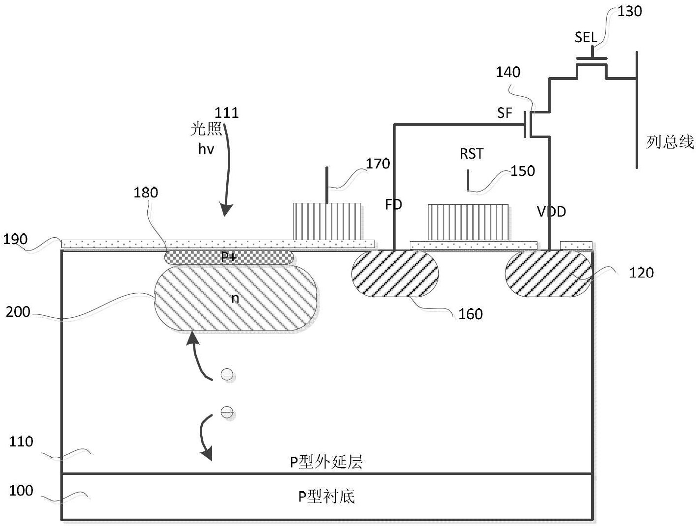
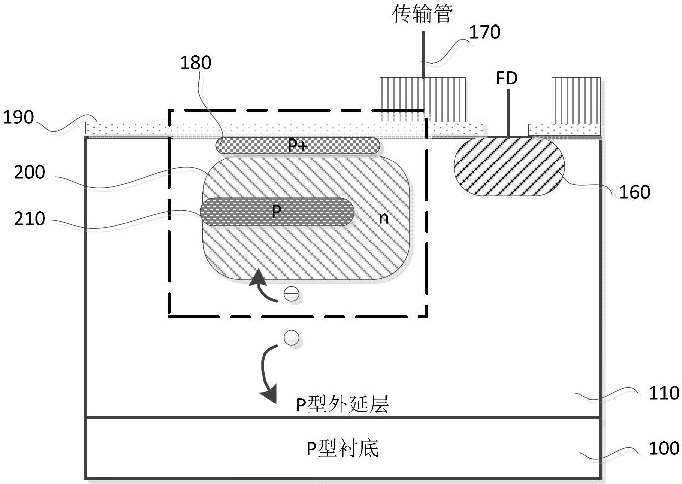
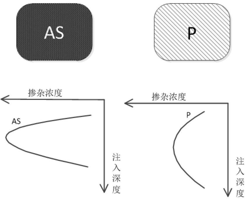
[0024] The present invention is a structure optimization based on a layered PD structure, which is used to improve the full well capacity and dynamic range of small pixels without increasing the dark current when designing a small pixel image sensor. In the traditional PPD and the unimproved hierarchical PPD structure ( figure 1 and figure 2), the N-buried layer 200 is realized by a single N-type doping of the same type, such as phosphorus (P) or arsenic (AS). For the N buried layer doped with phosphorus (P), because P has a relatively high diffusion coefficient during ion implantation, the concentration distribution curve of the N buried layer formed by implantation is easy to form with a lower concentration and a wider range. Large doping concentration distribution, that is, "flat and wide", such as image 3 Shown in B. However, if in order to increase the full well capacity of the small pixel, only a higher dose of AS doping implantation is used to form the N buried lay...


PUM


Abstract

The invention relates to a complementary metal oxide semiconductor (CMOS) solid image sensor, and provides a small-size CMOS image sensor pixel photodiode structure, which ensures that an optimized small pixel unit can increase full-trap capacity under the condition of no increase of dark current, therefore dynamic range, signal to noise ratio and the like are indirectly increased, and the optimal design of the small pixel unit is completed. In order to achieve the purpose, the technical scheme adopted by the invention is as follows:, according to the small-size CMOS image sensor pixel photodiode structure, a pixel photodiode is formed by injecting a shallower N type region buried layer on a P type epitaxial layer, an N type region is of a U type buried layer structure formed by homotype impurities with larger diffusion coefficients, the middle of the U type buried layer structure is provided with homotype impurities with smaller diffusion coefficients; and an impurity injection layerwith a larger diffusion coefficient completely buries an impurity injection layer with smaller diffusion coefficient. The invention is mainly used for designing and manufacturing the CMOS solid imagesensor.

Description

technical field [0001] The present invention relates to a metal complementary oxide semiconductor (CMOS) solid-state image sensor, in particular, to a photodiode structure of a small-sized CMOS image sensor pixel. Background technique [0002] Image sensors are semiconductor devices that convert incident light signals into electrical signals. According to different working principles, it is mainly divided into two categories: charge coupled image sensor (Charge Coupled Device) and CMOS image sensor (complementary metal-oxide-semiconductor). In recent years, benefiting from the rapid progress of standard CMOS technology and the continuous reduction of feature size, CMOS image sensors can be integrated with more digital-analog circuits on the same chip, realizing low power consumption, low cost, high integration and other CCD The incomparable advantages of image sensors have also promoted the rapid development of CMOS image sensors in recent years. [0003] A CMOS image sens...

Claims


Application Information

Patent Timeline
IPC IPC(8): H01L27/146
Inventor 姚素英孙羽高静徐江涛史再峰高志远
Owner TIANJIN UNIV
Why Eureka
Try Eureka