
Multi-stage exchange system and exchange method for multi-station silicon wafer stage

A technology of exchange system and wafer table, applied in multi-station wafer table multi-table exchange system and its workflow field, can solve the problems of increasing work area and production cost, reducing silicon wafer processing efficiency, etc., and achieve cost reduction and the use of area, the effect of improving productivity and accuracy

Active Publication Date: 2012-09-19
TSINGHUA UNIV +1
View PDF8 Cites 15 Cited by
  • Summary
  • Abstract
  • Description
  • Claims
  • Application Information

AI Technical Summary

Problems solved by technology

In the process of photolithography of silicon wafers using the existing dual-stage exchange lithography machine, since the wafer stage system only has two stations, the measurement station and the exposure station, all of which are equipped with measurement and alignment instruments and auxiliary parts, the exposure station The position is also equipped with an exposure system, which is not convenient for process processing. It is necessary to take out the silicon wafer from the lithography machine and perform the above process outside the lithography machine, which reduces the processing efficiency of the silicon wafer; There will be errors between the benchmark determined during alignment in the lithography machine and the benchmark determined during the previous alignment; when performing double exposure processing, two lithography machines need to work together, which increases the work area and production cost

Method used


Image

  • Multi-stage exchange system and exchange method for multi-station silicon wafer stage
  • Multi-stage exchange system and exchange method for multi-station silicon wafer stage
  • Multi-stage exchange system and exchange method for multi-station silicon wafer stage

Examples


Embodiment Construction

[0027] The principle, structure and implementation of the present invention will be further described in detail below in conjunction with the accompanying drawings.

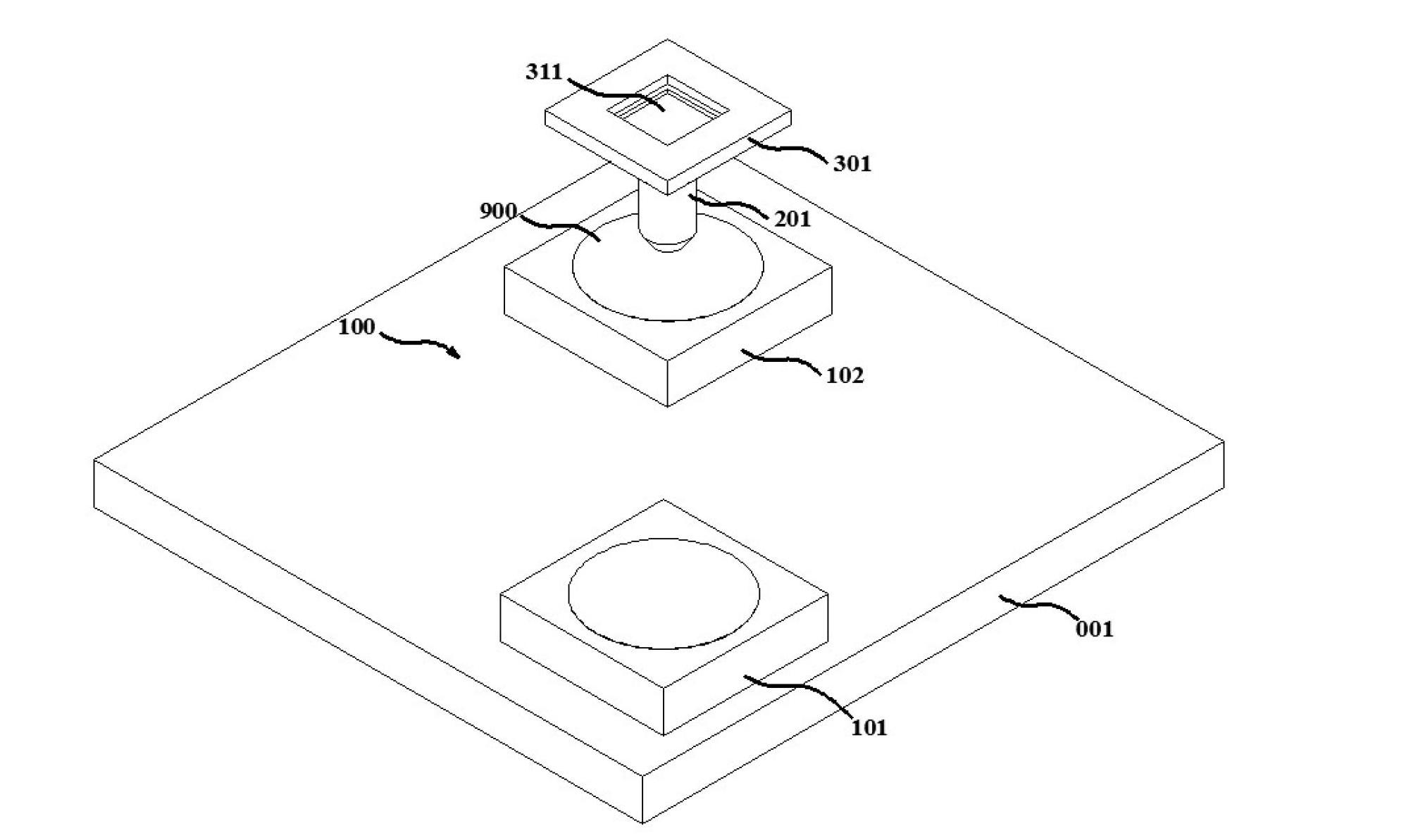
[0028] figure 1 It is a two-station silicon wafer platform dual-station exchange system in the existing dual-station exchange lithography machine, including the base station 001, the measurement station 101, the exposure station 102 and two wafer holders for carrying silicon wafers 900; the base station The upper surface 100 of the stage is an air-floating plane or a magnetic-floating plane, and the measuring station and the exposure station are located on the upper surface of the base; Complete the exchange between the measurement station and the exposure station. The existing two-station silicon wafer exchange system has only two stations, the measurement station and the exposure station, both of which are equipped with measurement and alignment instruments and auxiliary parts. The exposure station is also equ...


PUM


Abstract

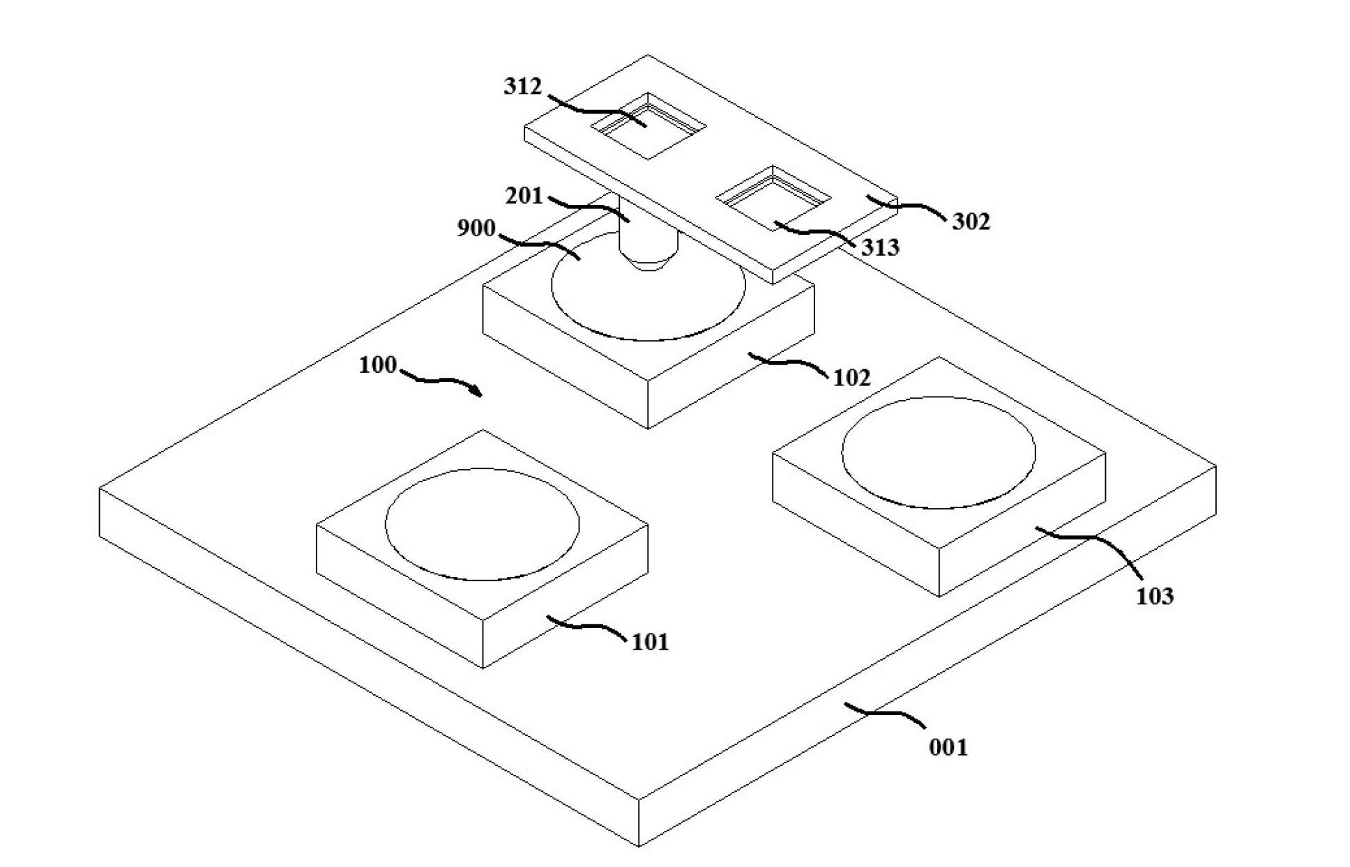
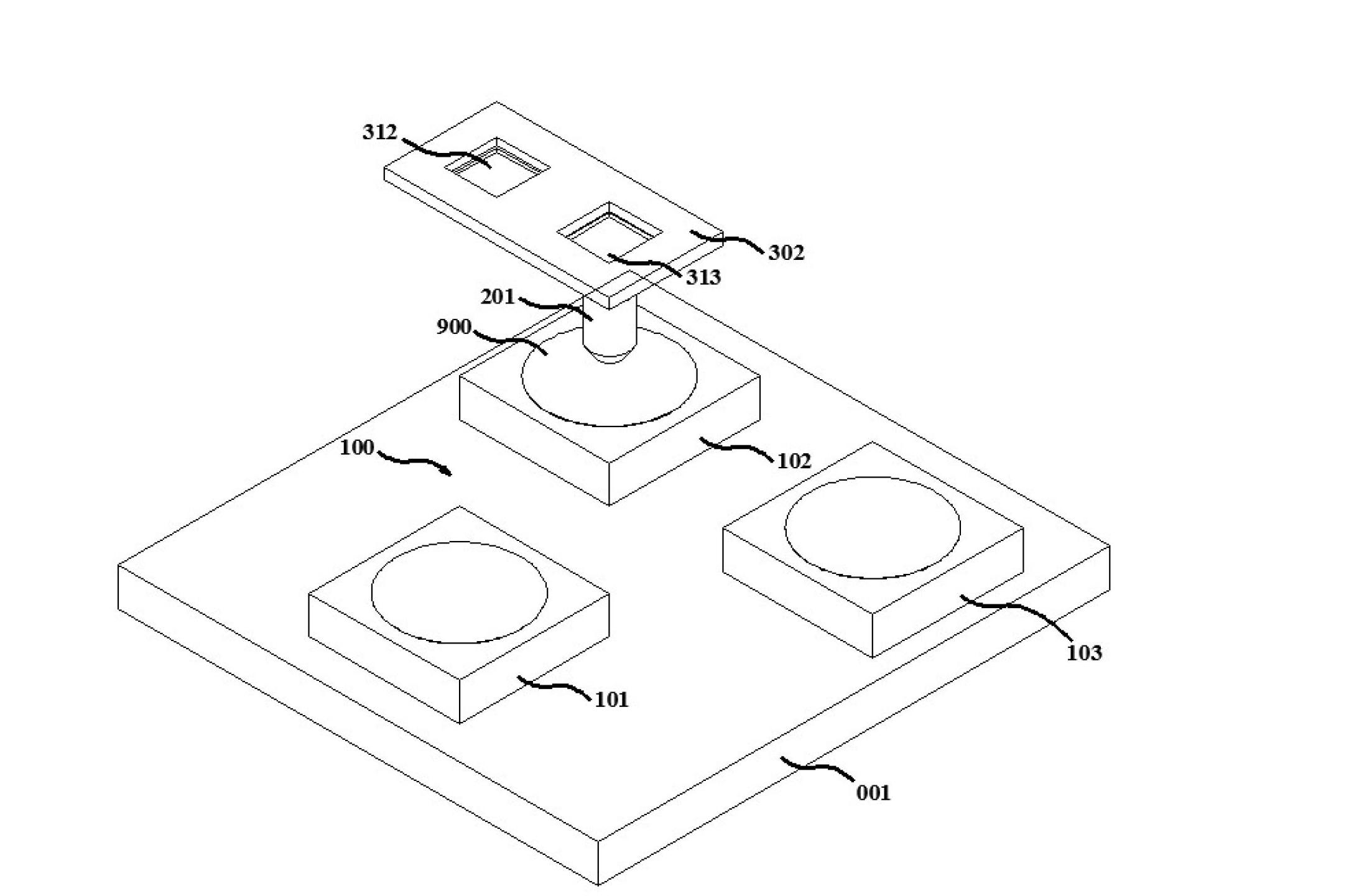
The invention discloses a multi-stage exchange system and a multi-stage exchange method for a multi-station silicon wafer stage. The multi-stage exchange system comprises a measurement station, an exposure station and a process treatment station, wherein the process treatment station, the measurement station and the exposure station are all positioned in an air floatation plane or a magnetic suspension plane on the upper surface of a base stage; and a wafer carrying stage is arranged on the upper surface of the base stage through an air floatation bearing or magnetic suspension, carries a silicon wafer and is driven by a linear motor or a planar motor to finish exchange of all stations. By adding the process treatment station, the process treatment of two adjacent exposure procedures can be realized in a photo-etching machine, and an exposure procedure and a process treatment procedure can be concurrently finished in the same photo-etching machine, so continuous exposure is realized in the same photo-etching machine, and requirements for improving productivity and accuracy and reducing cost and using area in a dual-exposure technology or even a multi-exposure technology are met.

Description

technical field [0001] The invention relates to a multi-station silicon wafer platform multiple exchange system and its work flow, which are mainly used in the technical field of semiconductor manufacturing. Background technique [0002] In semiconductor manufacturing, with the gradual reduction of the size of semiconductor devices, the pattern feature size is getting closer to the limit of photolithography processing methods, distributing layout patterns on one or more masks and multiple processing of silicon wafers. The method of sub-exposure and etching has been used more and more. [0003] When the feature size of the pattern approaches the limit of the photolithographic processing method, it is necessary to replace a higher-performance projection system and projection radiation beam, which makes it difficult to develop equipment and greatly increases the processing cost of semiconductor devices. On the basis of existing equipment, the exposure resolution can be doubled...

Claims


Application Information

Patent Timeline
IPC IPC(8): G03F7/20
Inventor 朱煜张鸣支凡刘昊刘召徐登峰杨开明胡金春尹文生
Owner TSINGHUA UNIV
Learn More