
Forming method of performing forming on variable resistance nonvolatile memory element, and variable resistance nonvolatile memory device

A non-volatile storage, resistance change technology, applied in electrical components, information storage, static memory, etc., can solve the problems of reduced cell current, uneven voltage formed by resistance change elements, and increased voltage formed by resistance change elements.

Active Publication Date: 2012-09-12
PANASONIC SEMICON SOLUTIONS CO LTD
View PDF7 Cites 13 Cited by
  • Summary
  • Abstract
  • Description
  • Claims
  • Application Information

AI Technical Summary

Problems solved by technology

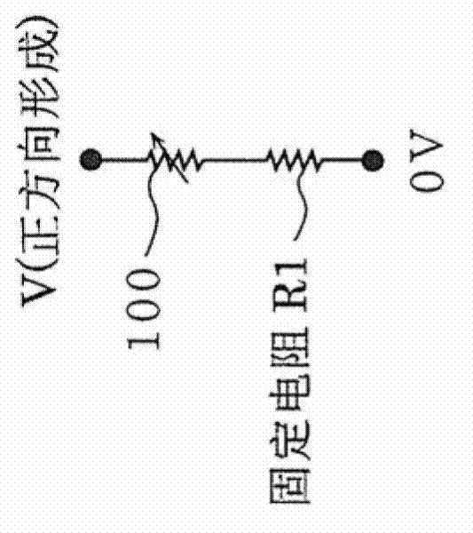
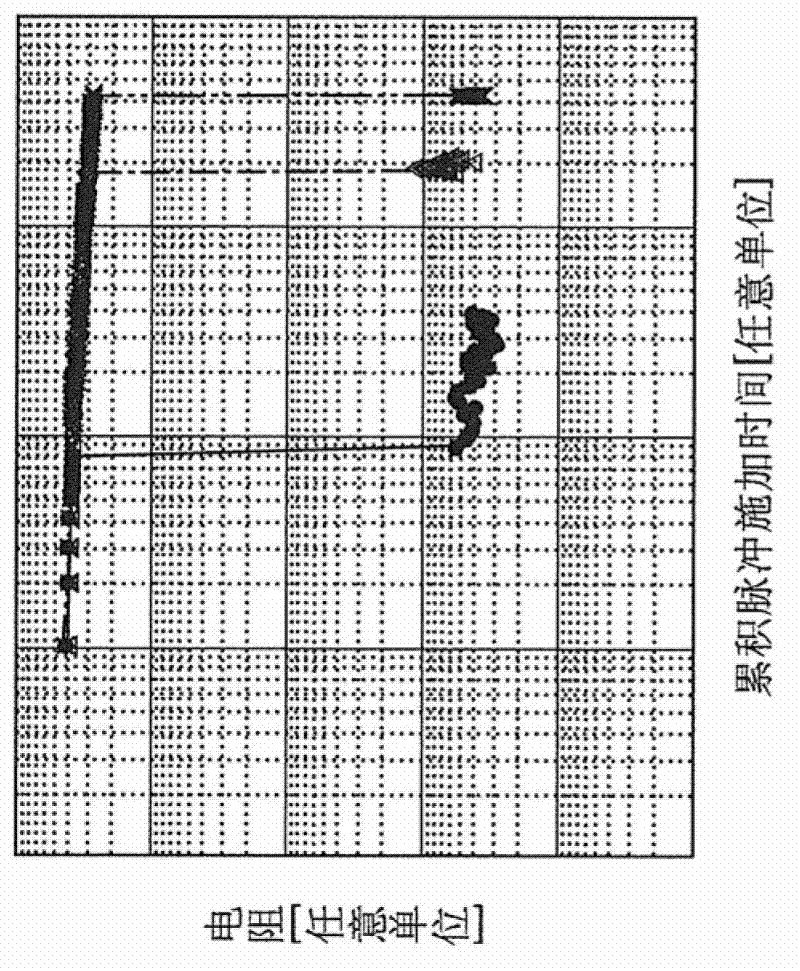
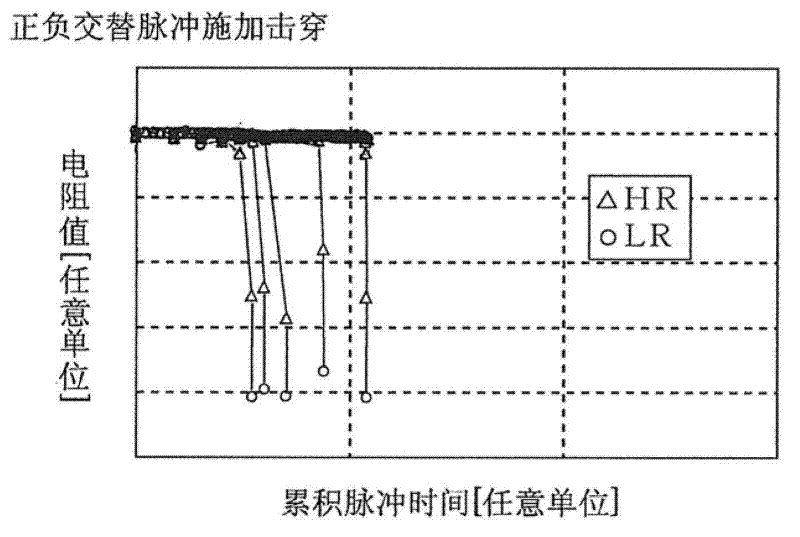
[0045] However, the above-mentioned conventional resistance variable semiconductor memory device has a problem that the formation voltage is not uniform for each resistance variable element constituting the memory cell array, or that the initial voltage applied to the resistance to transition to the state where the resistance change starts is The formation voltage of the change element becomes higher
In addition, although it will be described in detail later, it is clear that there is another problem in the formation method according to the related invention for solving such a problem that the cell current in the low-resistance state decreases (that is, the low resistance of the resistance variable element Insufficient resistance value in the state becomes low)

Method used


Image

  • Forming method of performing forming on variable resistance nonvolatile memory element, and variable resistance nonvolatile memory device
  • Forming method of performing forming on variable resistance nonvolatile memory element, and variable resistance nonvolatile memory device
  • Forming method of performing forming on variable resistance nonvolatile memory element, and variable resistance nonvolatile memory device

Examples


no. 2 Embodiment approach

[0284] Next, the description implements Figure 16 An example of the nonvolatile memory device of the formation flow is taken as the second embodiment of the present invention.

[0285] (Nonvolatile memory device according to the second embodiment)

[0286] Figure 19It is a block diagram showing an example of the configuration of the variable resistance nonvolatile memory device 200 (hereinafter, simply referred to as the nonvolatile memory device 200 ) according to the second embodiment of the present invention. and, Figure 20 is showing Figure 19 A perspective view of the structure of part A (the structure of the 4-bit part) in .

[0287] like Figure 19 It is shown that the nonvolatile memory device 200 according to this embodiment includes a memory main body 201 on a semiconductor substrate, and the memory main body 201 includes: a memory cell array 202; a row selection circuit / driver 203; a column selection circuit / driver 204; The writing circuit 205 is used to w...

no. 3 Embodiment approach

[0370] Next, the third embodiment of the present invention will describe a case in which the automatic formation control circuit 211 and the automatic formation circuit 210 in the nonvolatile memory device described in the second embodiment are not provided in the device, and from The outside of the nonvolatile memory device is controlled and implemented.

[0371] (Nonvolatile memory device according to the third embodiment)

[0372] Figure 26 It is a block diagram showing an example of the configuration of the variable resistance nonvolatile memory device 400 (hereinafter, simply referred to as the nonvolatile memory device 400 ) according to the embodiment of the present invention.

[0373] like Figure 26 As shown, the nonvolatile memory device 400 according to this embodiment includes a memory main body 401 on a semiconductor substrate, and the memory main body 401 includes a memory cell array 402 for Figure 39 The illustrated upper electrode 100c utilizes 1T1R type m...


PUM

PropertyMeasurementUnit
Film thicknessaaaaaaaaaa

Abstract

In forming, an automatic forming circuit (210) included in a nonvolatile memory device (200) causes a constant current IL to flow in a selected memory cell having a considerably high initial resistance. When the forming generates a filament path in the memory cell and thereby a resistance value is decreased, a potential of a node NBL and a potential of a node Nin are also decreased. If the potentials become lower than that of a reference voltage Vref, an output NO of a difference amplifier (303) for detecting forming success is activated, and a forming success signal Vfp is activated after a delay time depending on the number n of flip flops FF1 to FFn and a clock signal CLK. Thereby, a switch transistor (301) is in a non-conducting state and the forming on a variable resistance element is automatically terminated.

Description

technical field [0001] The present invention relates to a method for forming (initializing) a variable resistance nonvolatile memory element whose resistance value is reversibly changed in response to an electric signal to stably change resistance, and a variable resistance nonvolatile memory having that function device. Background technique [0002] In recent years, variable resistance nonvolatile memory devices (hereinafter also simply referred to as "Non-volatile memory device".) research and development. The so-called variable resistance element refers to an element that has the property that the resistance value changes reversibly according to an electric signal, and can store data corresponding to the resistance value in a non-volatile manner. [0003] As a nonvolatile memory device using a variable resistance element, a nonvolatile memory device in which so-called 1T1R type memory cells are arranged in a matrix is ​​generally known. A MOS transistor and a variable ...

Claims


Application Information

Patent Timeline
IPC IPC(8): G11C13/00H01L27/10H01L27/105H01L45/00H01L49/00
CPCG11C13/0007G11C2013/0083G11C13/0064G11C13/0069G11C2013/0073G11C2213/32G11C2213/72G11C2213/79H10B63/20H10N70/24H10N70/826H10N70/8833H01L27/101
Inventor 河合贤岛川一彦片山幸治村冈俊作
Owner PANASONIC SEMICON SOLUTIONS CO LTD
Learn More