Plasma excimer gain waveguide
A plasmon and waveguide technology, which is applied in the field of optical waveguides, can solve the problems of weakened coupling between gain waveguides and metal plasmons, poor optical locality, and reduced threshold gain, so as to achieve long propagation distance and increase propagation distance. , improve the local effect
- Summary
- Abstract
- Description
- Claims
- Application Information
AI Technical Summary
Problems solved by technology
Method used
Image
Examples
Embodiment 1
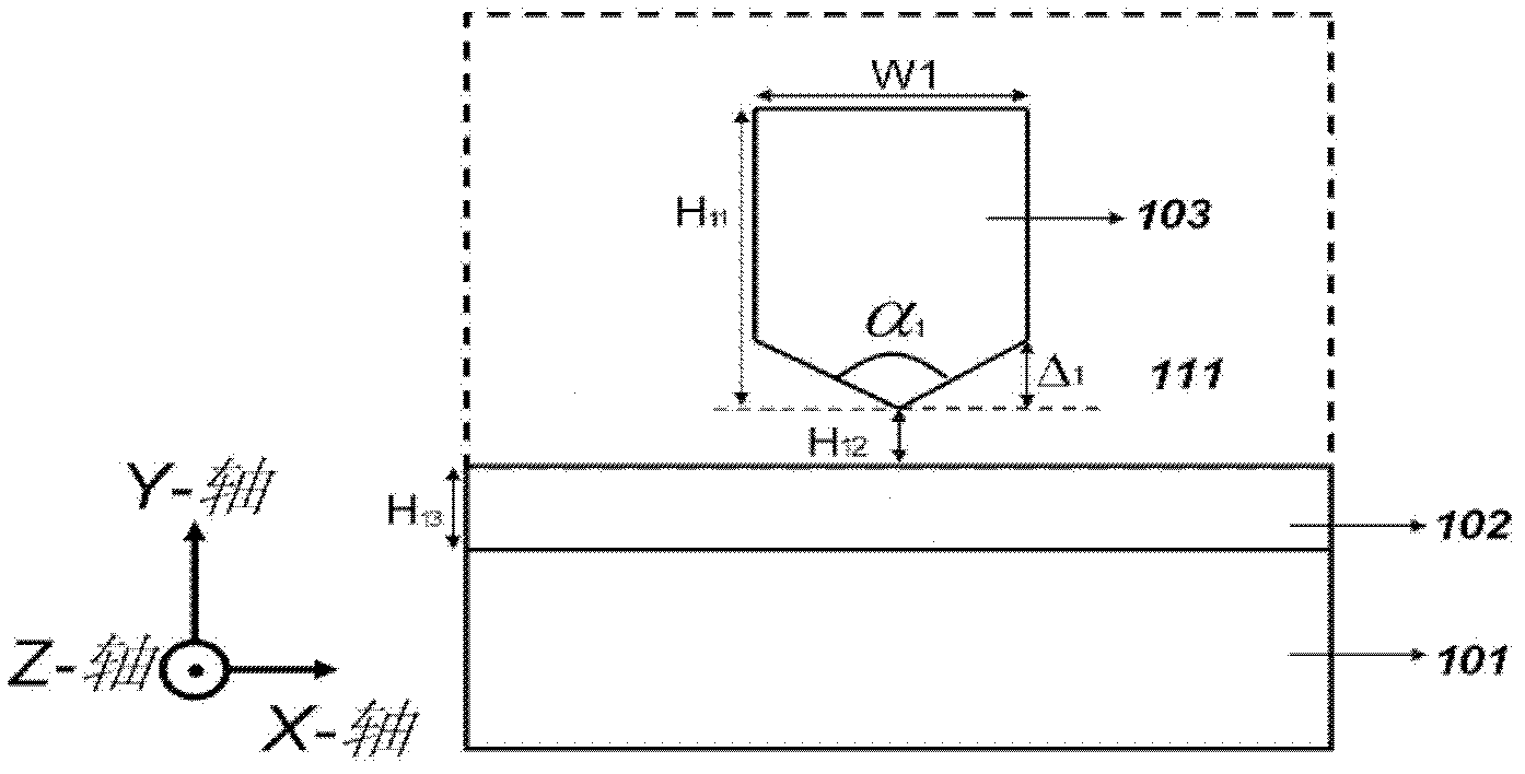
[0045] figure 1 Shown is a structural diagram of Embodiment 1 of a plasmon gain waveguide provided by the present invention. figure 1 Among them, the x-axis, y-axis and z-axis respectively represent the coordinate axes x-axis, y-axis and z-axis, the direction of the z-axis is perpendicular to the surface of the figure, and the positive direction of the z-axis is outward.
[0046] The first embodiment provides a plasmon gain waveguide 103, including a base layer 101, a dielectric layer 102, an isolation layer 111 and a gain waveguide 103, the dielectric layer 102 is placed on the exposed surface of the base layer 101, and the isolation layer 111 Between the dielectric layer 102 and the gain waveguide 103, the end of the gain waveguide 103 close to the dielectric layer 102 is wedge-shaped and the tip faces the dielectric layer 102, and the refractive index of the gain waveguide 103 is greater than the The refractive index of the isolation layer 111 is described above.
[0047]...
Embodiment 2
[0064] Figure 9 Shown is a structural diagram of Embodiment 2 of a plasmon gain waveguide provided by the present invention. Figure 9 Among them, the x-axis, y-axis and z-axis respectively represent the coordinate axes x-axis, y-axis and z-axis, the direction of the z-axis is perpendicular to the surface of the figure, and the positive direction of the z-axis is outward.
[0065] This embodiment provides a plasmon gain waveguide 903, which includes a base layer 901, a dielectric layer 902, an isolation layer 904, and a gain waveguide 903. The dielectric layer 902 is placed on the exposed surface of the base layer 101, and the isolation layer 904 mediates Between the dielectric layer 902 and the gain waveguide 903, one end of the gain waveguide 903 close to the dielectric layer 902 is wedge-shaped with the tip facing the dielectric layer 902, and the refractive index of the gain waveguide 903 is larger than the The refractive index of the isolation layer 904 .
[0066] Fi...
PUM
 Abstract
Description
Claims
Application Information
 - Generate Ideas
- Intellectual Property
- Life Sciences
- Materials
- Tech Scout
- Unparalleled Data Quality
- Higher Quality Content
- 60% Fewer Hallucinations
Browse by: Latest US Patents, China's latest patents, Technical Efficacy Thesaurus, Application Domain, Technology Topic, Popular Technical Reports.
© 2025 PatSnap. All rights reserved.Legal|Privacy policy|Modern Slavery Act Transparency Statement|Sitemap|About US| Contact US: help@patsnap.com


