Monolithic reference full bridge magnetic field sensor
A magnetic field sensor, monolithic technology, applied in the field of sensors, can solve the problems of low-cost mass production and difficulty in achieving consistent matching of magnetoresistive output
- Summary
- Abstract
- Description
- Claims
- Application Information
AI Technical Summary
Problems solved by technology
Method used
Image
Examples
no. 3 example
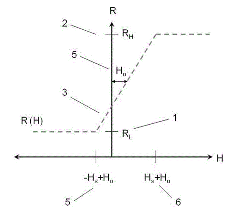
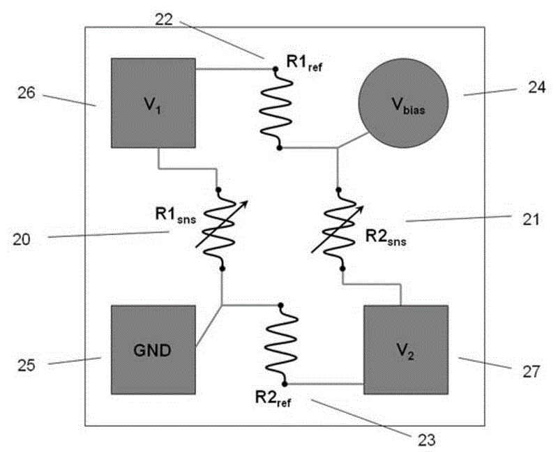
[0090] In the third embodiment of the present invention, a single-chip reference full-bridge magnetic field sensor includes two reference arms and two sensing arms, and the two reference arms and the two sensing arms are connected at intervals to form a full bridge, each A bridge arm resistance is composed of one or more MTJ or GMR magneto-resistance elements; the MTJ or GMR magneto-resistance elements use the linear part of their output curves to induce magnetic fields; the magnetic field sensor also includes a wrapping reference arm The shielding layer of the magnetoresistive element, the shielding layer is a ferromagnetic material with high magnetic permeability; the pad of the magnetic field sensor can be connected to the packaging pin of the ASIC integrated circuit or the lead frame through a lead wire.
[0091] Preferably, the reference arm includes one or more magnetoresistive elements connected in series to adjust the resistance of the reference arm, and the sensing ...
no. 4 example
[0092] In the fourth embodiment of the present invention, a single-chip reference full-bridge magnetic field sensor includes two reference arms and two sensing arms, and the two reference arms and the two sensing arms are connected at intervals to form a full bridge Bridge, the reference arm and the sensing arm are composed of one or more MTJ or GMR magnetoresistive elements; the MTJ or GMR magnetoresistance elements use the linear part of their output curves to induce magnetic fields; the upper layer of the free layer of the reference arm element Or a layer of antiferromagnetic layer or permanent magnetic layer is deposited on the lower layer, and the reference arm is biased by using the exchange coupling of the antiferromagnetic layer or the exchange coupling and scattered field coupling of the permanent magnetic layer; the pad of the magnetic field sensor Can be wire-connected to the package pins of an ASIC integrated circuit or a lead frame.
[0093] Preferably, the mag...
PUM
 Abstract
Description
Claims
Application Information
 - R&D
- Intellectual Property
- Life Sciences
- Materials
- Tech Scout
- Unparalleled Data Quality
- Higher Quality Content
- 60% Fewer Hallucinations
Browse by: Latest US Patents, China's latest patents, Technical Efficacy Thesaurus, Application Domain, Technology Topic, Popular Technical Reports.
© 2025 PatSnap. All rights reserved.Legal|Privacy policy|Modern Slavery Act Transparency Statement|Sitemap|About US| Contact US: help@patsnap.com


