
Heat radiation plate, semiconductor device and manufacturing method of heat radiation plate

A manufacturing method and heat dissipation plate technology, which are applied in semiconductor/solid-state device manufacturing, semiconductor devices, semiconductor/solid-state device components, etc., can solve problems such as reduced jointability, cracks, and inability to bond semiconductor elements well, and achieve improved The effect of bonding reliability

Inactive Publication Date: 2012-07-18
MITSUBISHI MATERIALS CORP
View PDF3 Cites 12 Cited by
  • Summary
  • Abstract
  • Description
  • Claims
  • Application Information

AI Technical Summary

Problems solved by technology

[0012] However, as mentioned above, when the metal surface layer is formed by eluting the metal impregnated in the carbonaceous part on the sheet surface of the metal matrix composite material, it is difficult to form the metal surface layer uniformly, and good bonding may not be possible. Heating elements such as semiconductor elements
In addition, since the metal surface layer is formed by impregnating the metal in the carbonaceous part, there is a problem that the material of the metal surface layer cannot be changed.
[0013] On the other hand, in the case where the metal surface layer is formed by electroplating or vacuum evaporation on the surface of the metal matrix composite material, although the material of the metal surface layer can be made different from the metal impregnated in the carbonaceous part, it is possible to reduce the metal surface layer. The bondability between the surface layer and the metal matrix composite material plate surface may not be able to bond well with heating elements such as semiconductor elements
[0014] In addition, when the metal surface is formed by plating, tensile stress remains on the metal surface, and cracks are likely to occur when the metal surface deteriorates, which may cause trouble for bonding with heating elements such as semiconductor elements.
[0015] Furthermore, in the case of vacuum deposition, a lot of labor is required to form the metal surface layer, and there is a problem that the manufacturing cost of the heat sink greatly increases.

Method used


Image

  • Heat radiation plate, semiconductor device and manufacturing method of heat radiation plate
  • Heat radiation plate, semiconductor device and manufacturing method of heat radiation plate
  • Heat radiation plate, semiconductor device and manufacturing method of heat radiation plate

Examples


Embodiment Construction

[0057] Hereinafter, embodiments of the present invention will be described with reference to the drawings.

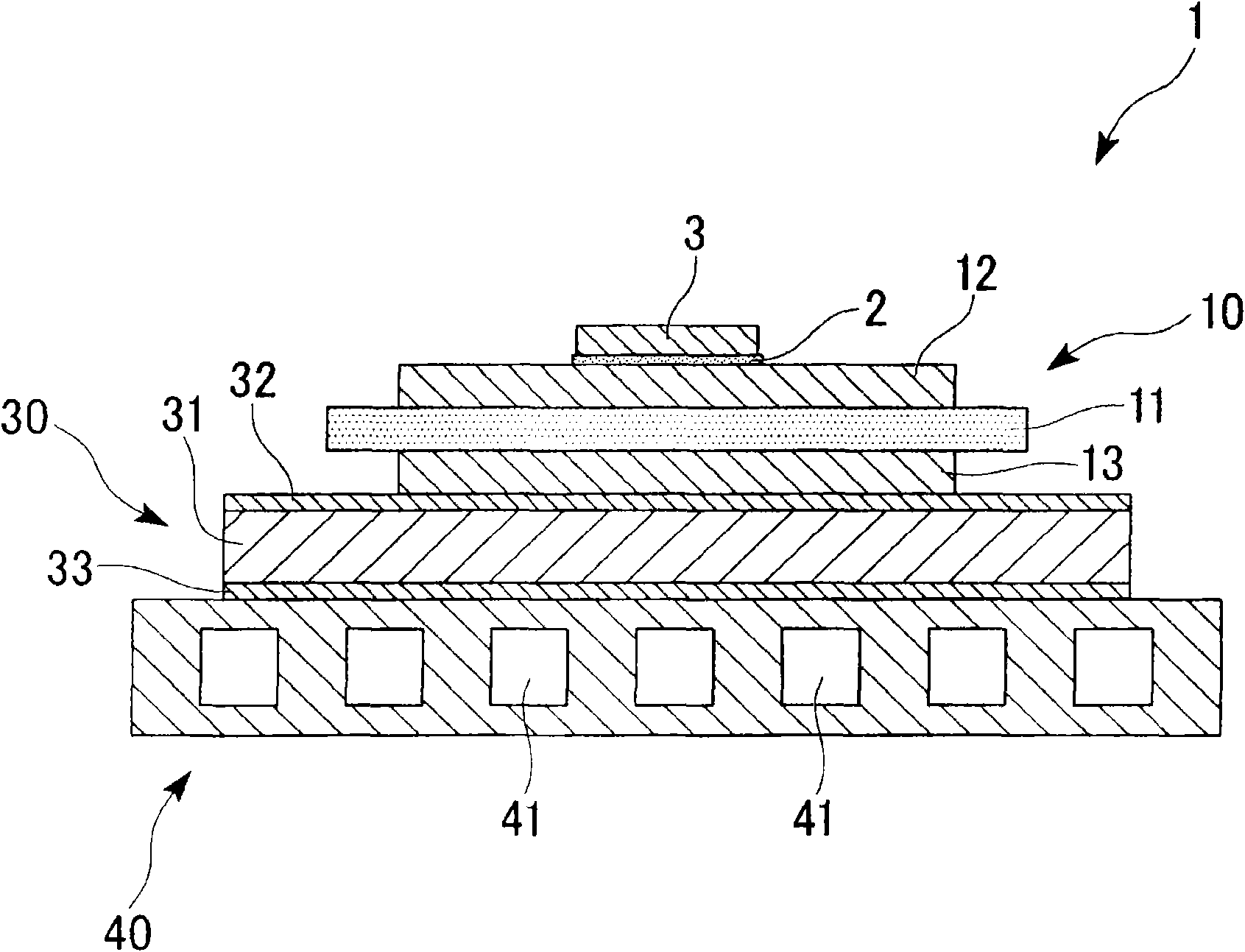
[0058] First, refer to Figure 1 to Figure 4 , a power module (semiconductor device) using the heat sink according to the first embodiment of the present invention will be described.

[0059] figure 1 The illustrated power module 1 includes a power module substrate 10, and on one side of the power module substrate 10 (in figure 1 The upper side in the center) the semiconductor chip 3 bonded by the solder layer 2 is arranged on the other side of the power module substrate 10 (on the figure 1 The center is the lower side) of the heat sink 30 and the cooler 40 arranged on the other side of the heat sink.

[0060] The power module substrate 10 includes a ceramic substrate 11, and is disposed on one side of the ceramic substrate 11 (in figure 1 The circuit layer 12 on the top) and the other side of the ceramic substrate 11 (in the figure 1 The middle is the metal layer ...


PUM

PropertyMeasurementUnit
particle diameteraaaaaaaaaa
flexural strengthaaaaaaaaaa

Abstract

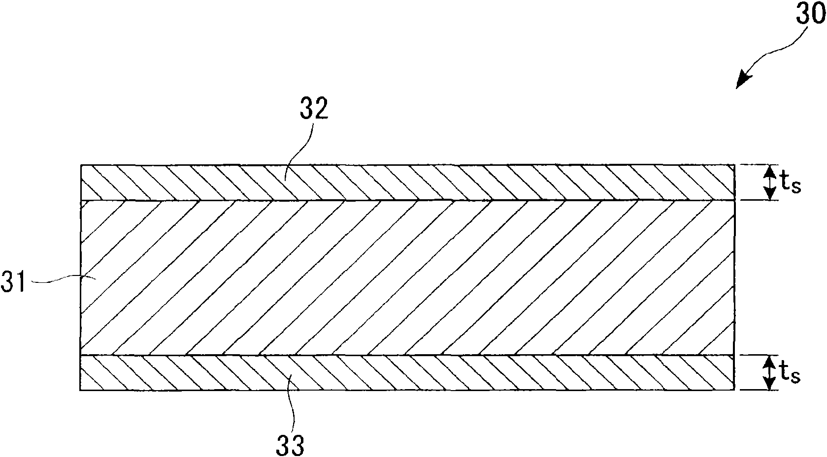
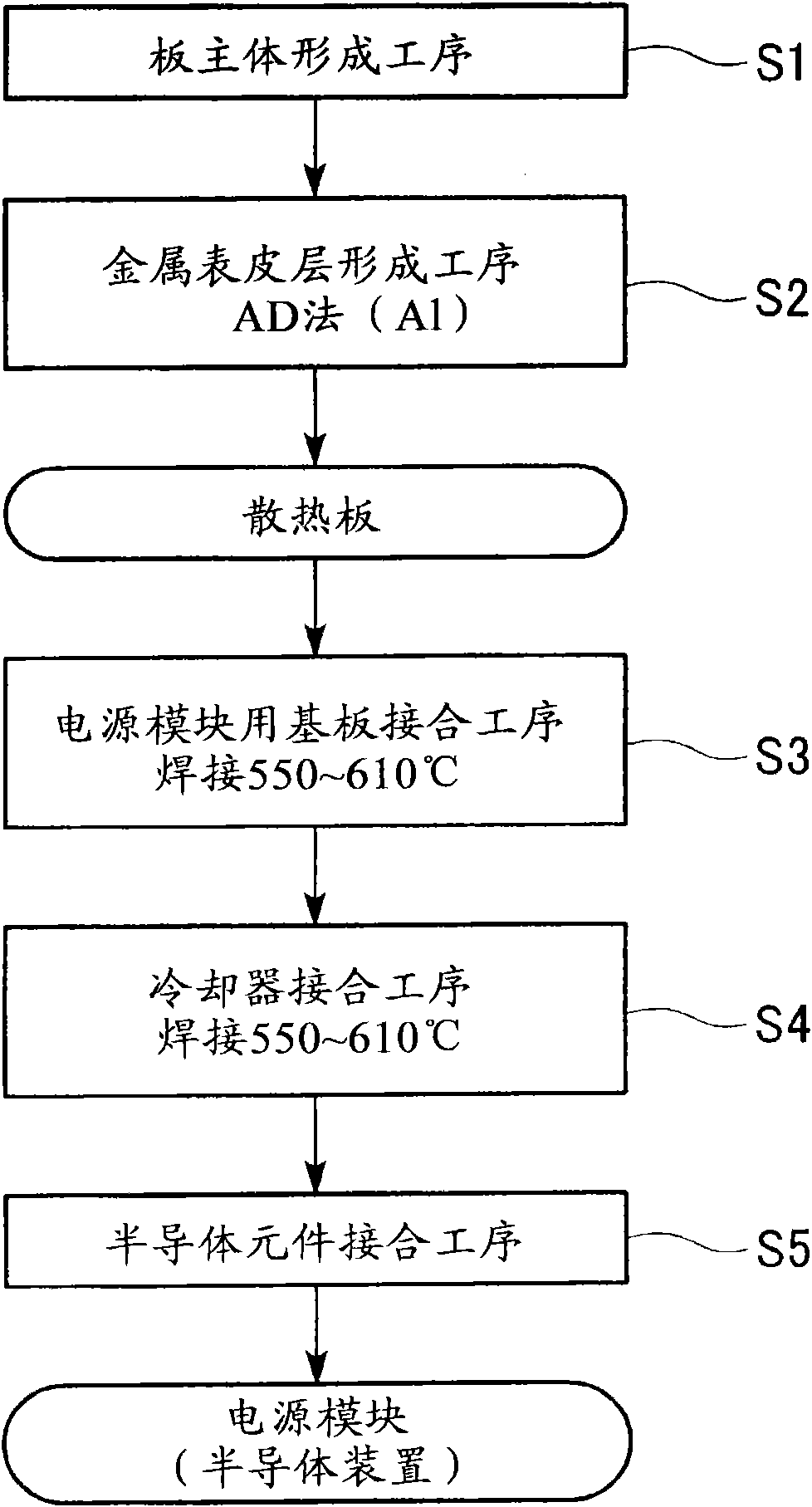
The invention provides a heat radiation plate which has an excellent heat radiation property and can prevent the heat stress from acting on heating bodies such as a semiconductor element under a cold and hot circulating load, a semiconductor device utilizing the heat radiation plate and a manufacturing method of the heat radiation plate. The heat radiation plate (30) is used for radiating heat produced by a heating body (3) which is carried by the heat radiation plate (30); and the heat radiation plate (30) is characterized by having a plate main body (31) and metal surface layers (32 and 33), wherein the plate main body (31) is formed by filling a metal-based composite material of a metal material into a carbon part, the metal surface layers (32 and 33) are formed on at least one side surface of the plate main body (31), the metal-based composite material forming the plate main body is formed by impregnating a molten metal material into the carbon part, and the metal surface layers (32 and 33) are formed through collision of metal powder onto the surfaces of the plate main body (31).

Description

technical field [0001] The present invention relates to a heat sink mounted with a heat generating body such as a semiconductor element and dissipating heat generated from the heat generating body, a semiconductor device including the heat sink, and a method for manufacturing the heat sink. Background technique [0002] In recent years, the heat generated from electronic devices tends to increase along with higher functionality, larger capacity, and miniaturization of electronic devices. Therefore, it is required to efficiently dissipate the heat. [0003] For example, in a semiconductor device mounted with a semiconductor element as a heat generating body, as disclosed in Patent Document 1, a heat sink having good thermal conductivity is used to diffuse heat generated from the semiconductor. [0004] In addition, since the mounted semiconductor elements are made of, for example, Si etc. and have a relatively small coefficient of thermal expansion, the heat sink used in the ...

Claims


Application Information

Patent Timeline
Patent Type & Authority Applications(China)
IPC IPC(8): H01L23/367H01L23/373H01L21/48H01L21/20C23C24/04
CPCH01L2924/0002H01L2224/32225
Inventor 长濑敏之长友义幸黑光祥郎
Owner MITSUBISHI MATERIALS CORP
Learn More