Multilayer spacer type IC (Integrated Circuit) chip stacked package of substrate and production method of package
A chip stacking and packaging technology, applied in the field of multi-layer spacer IC chip stacking and packaging, can solve problems such as poor insulation performance, affecting the height of bonding wires connecting IC chips and carrier pads, affecting chip heat dissipation, etc. , to achieve the effect of facilitating heat dissipation, solving height problems, and improving insulation performance
- Summary
- Abstract
- Description
- Claims
- Application Information
AI Technical Summary
Problems solved by technology
Method used
Image


Examples
Embodiment 1
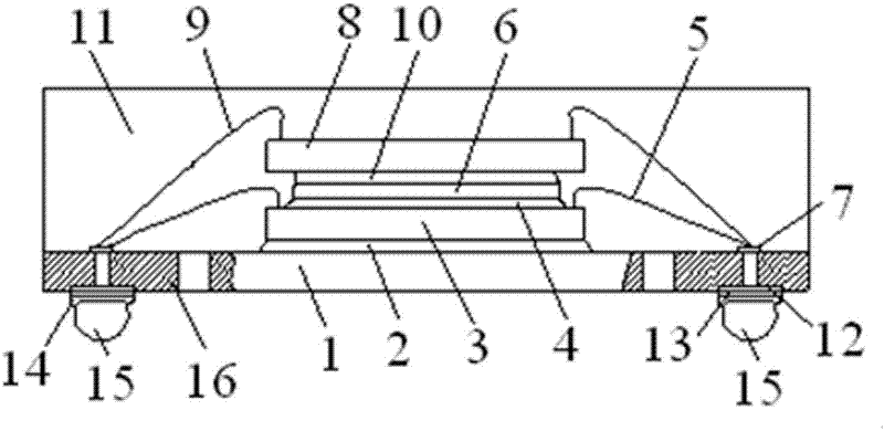
[0104]The thickness of the chip thickness from the thickness of the original wafer to the final thickness of 100 μm; the thickness of the rough grinding range from the thickness of the original wafer to 150 μm +the thickness of the glue film, the thick grinding speed of 2 μm / s;The thickness of the glue membrane, the fine grinding speed is 0.6 μm / s, and the wafer thinning process is used to prevent the chip prevents warp; the roughness of the wafer after thinning is 0.10mm., Crack -proof chip processing software control technology, the speed of the cutter into the knife ≤10mm / s; the separation IC chip with a stretch membrane ring; the thinning single chip makes it the final thickness of 110 μm;From the original thickness of the single chip to 160 μm +the thickness of the glue film, the thick milling speed is 3 μm / s;The machine first on the carrier 1 of the BT substrate 16, and the upper -core machine automatically absorbs the first IC chip 3 on the electrical glue to bare the firs...
Embodiment 2
[0106] The thickness of the chip thickness from the thickness of the original wafer to the final thickness of 100 μm; the thickness of the rough grinding range from the thickness of the original wafer to 150 μm +the thickness of the glue film, the thick grinding speed of 5 μm / s;+The thickness of the glue membrane, 0.3 μm / s in the fine grinding speed, and the chip to prevent the chip's warpage process during the wafer thinning process; the roughness of the wafer after thinning is 0.05mm;Fragments and cracking chip processing software control technology, scratch the knife speed ≤10mm / s; obtain a separate IC chip with a stretch membrane ring.The thinning single chip makes its final thickness of 120 μm; During the thinning process of the single chip, the rough grinding range is from the original thickness of the single chip to 170 μm +the thickness of the glue film, and the thick grinding speed is 5 μm / s;By the thickness of 120 μm +glue film, the essence speed is 12 μm / s; the insulati...
Embodiment 3
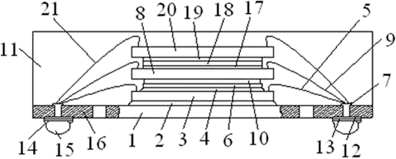
[0108] The thickness of the chip thickness is reduced from the thickness of the original wafer to the final thickness of 100 μm; the thickness of the rough grinding range from the thickness of the original wafer to 150 μm +the thickness of the glue film, the rough grinding speed is 3.5 μm / s;100 μm +glue film thickness, fine milling speed 0.45 μm / s, and the chip to prevent the chip's warpage process during the wafer thinning process;Film; use anti -fragmented, anti -cracking chip processing software control technology, the scratch in the knife is ≤10mm / s; obtains a separate IC chip with a stretch membrane ring; a thin single chip to make it final thickDuring the process, the rough grinding range ranged from the original thickness of the single chip to 150 μm +the thickness of the glue film, and the thick grinding speed was 4 μm / s;The insulating glue is first on the carrier 1 of the BT substrate 16 by the adhesive pinstonus.And use the anti -departure baking process for 175 ° C to ...
PUM
| Property | Measurement | Unit |
|---|---|---|
| Thickness | aaaaa | aaaaa |
| Flow length | aaaaa | aaaaa |
| Roughness | aaaaa | aaaaa |
Abstract
Description
Claims
Application Information
 - R&D
- Intellectual Property
- Life Sciences
- Materials
- Tech Scout
- Unparalleled Data Quality
- Higher Quality Content
- 60% Fewer Hallucinations
Browse by: Latest US Patents, China's latest patents, Technical Efficacy Thesaurus, Application Domain, Technology Topic, Popular Technical Reports.
© 2025 PatSnap. All rights reserved.Legal|Privacy policy|Modern Slavery Act Transparency Statement|Sitemap|About US| Contact US: help@patsnap.com