


Quick Research
Generate reliable direction feasibility study reports for your R&D in just a few steps.

Technical Q&A
Discover and master advanced knowledge NOW. Basics, ideas, possibilities, all at once.

Find Solutions
As an expert in R&D theories, this can generate solutions to your technical problems instantly.

Evaluate Feasibility
Analyze your overall solution with one click, know your potential R&D risks in advance.

Monitor Landscape
Get weekly tech updates, stay abreast of the latest tech innovations and key insights.
ldmos device and its manufacturing method
A device manufacturing method and epitaxial layer technology, applied in semiconductor/solid-state device manufacturing, semiconductor devices, electrical components, etc., can solve problems such as process defects and unclean silicon dioxide grinding, and achieve the effect of reducing process defects
- Summary
- Abstract
- Description
- Claims
- Application Information
AI Technical Summary
Problems solved by technology
Method used
Image

Examples
Embodiment 1
[0041] As mentioned in the background technology section, in the manufacturing process of LDMOS devices, the LOCOS process is often used to form a field oxide layer above the drift region, and the field oxide layer is generally used as an isolation layer for devices in the active region (mostly high-voltage devices). However, the field oxide layer formed by the LOCOS process is difficult to apply to the process of 0.18 μm and below 0.18 μm due to the limitation of the “bird’s beak” effect; and after the field oxide layer is formed above the drift region, the field oxide layer About half of the thickness of the substrate is higher than the surface of the substrate, so a step is formed. The existence of the step prevents the subsequent CMP process from planarizing the substrate, resulting in process defects.
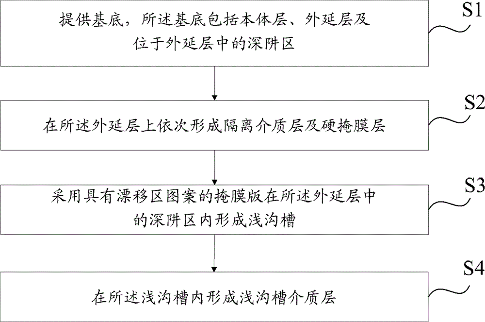
[0042] Based on this, the present invention provides a kind of LDMOS device manufacturing method, with reference to figure 1 , the method specifically includes the followi...
Embodiment 2
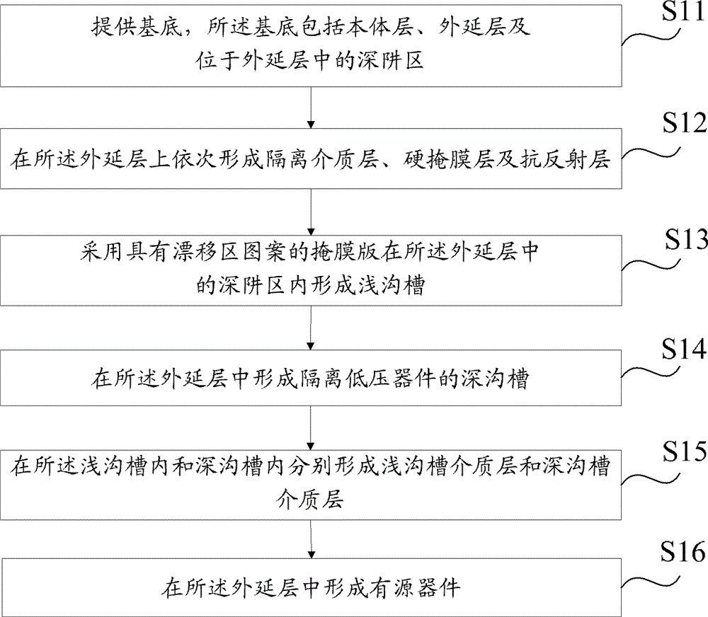
[0055] The LDMOS device manufacturing method provided by the present invention is described in detail below with a specific embodiment, refer to figure 2 , the method specifically includes the following steps:
[0056] Step S11: providing a substrate, the substrate includes a body layer, an epitaxial layer, and a deep well region in the epitaxial layer.
[0057] The "in the epitaxial layer" mentioned in this embodiment refers to a region extending downward from the surface of the epitaxial layer to a certain depth, which belongs to a part of the epitaxial layer; the "on the epitaxial layer" refers to the region upward from the surface of the epitaxial layer , this region does not belong to the epitaxial layer itself, and the meanings expressed in other descriptions can also be deduced by analogy.
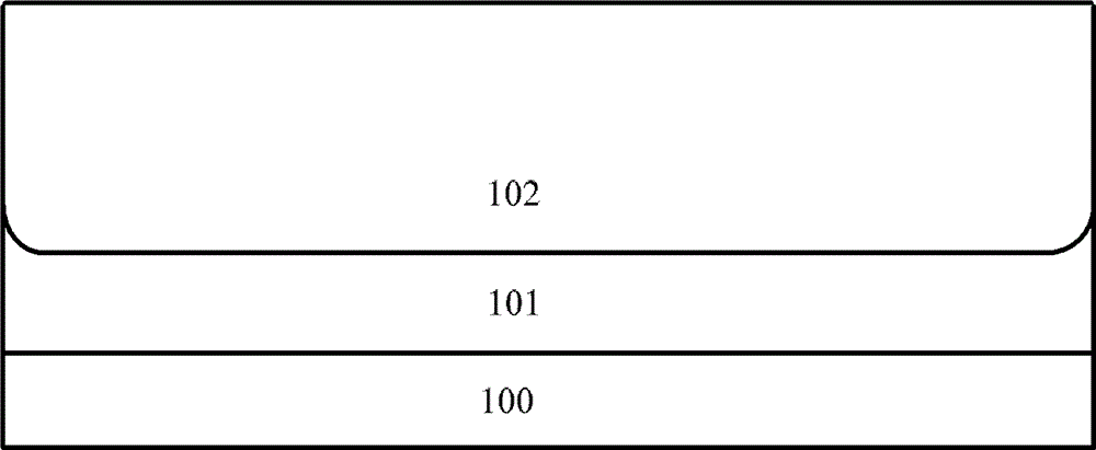
[0058] refer to image 3 , the figure shows a body layer 100 , an epitaxial layer 101 on the body layer 100 and a deep well region 102 in the epitaxial layer 101 .
[0059] In t...
Embodiment 3
[0087] The present invention also provides a kind of LDMOS device, refer to Figure 8 , the LDMOS device includes: a base, the base includes a body layer 100, an epitaxial layer 101, and a deep well region 102 located in the epitaxial layer 101; a first shallow trench dielectric layer 108 located in the deep well region 102 and The second shallow trench dielectric layer 109 .
[0088] The depths of the first shallow trench dielectric layer 108 and the second shallow trench dielectric layer 109 are both 100nm, and the sidewalls of the first shallow trench dielectric layer 108 and the second shallow trench dielectric layer 109 and the epitaxial The angle between the surface of the layer 101 is 80°-90°.
[0089] The formation process of the first shallow trench dielectric layer 108 and the second shallow trench dielectric layer 109 in the embodiment of the present invention is as follows: first, an isolation dielectric layer, a hard mask layer and an anti-reflection layer are se...
PUM
 Abstract
Description
Claims
Application Information
 - R&D Engineer
- R&D Manager
- IP Professional
- Industry Leading Data Capabilities
- Powerful AI technology
- Patent DNA Extraction
Browse by: Latest US Patents, China's latest patents, Technical Efficacy Thesaurus, Application Domain, Technology Topic, Popular Technical Reports.
© 2024 PatSnap. All rights reserved.Legal|Privacy policy|Modern Slavery Act Transparency Statement|Sitemap|About US| Contact US: help@patsnap.com