
Chemical mechanical grinding device

A technology of chemical machinery and grinding devices, which is applied in the direction of grinding devices, grinding machine tools, grinding tools, etc., can solve the problems of large detection errors, increasing influence, and great influence on measurement results, etc., achieving fast speed and improving The effect of timeliness and fast propagation speed of light waves

Inactive Publication Date: 2012-07-11
SEMICON MFG INT (SHANGHAI) CORP +1
View PDF8 Cites 4 Cited by
  • Summary
  • Abstract
  • Description
  • Claims
  • Application Information

AI Technical Summary

Problems solved by technology

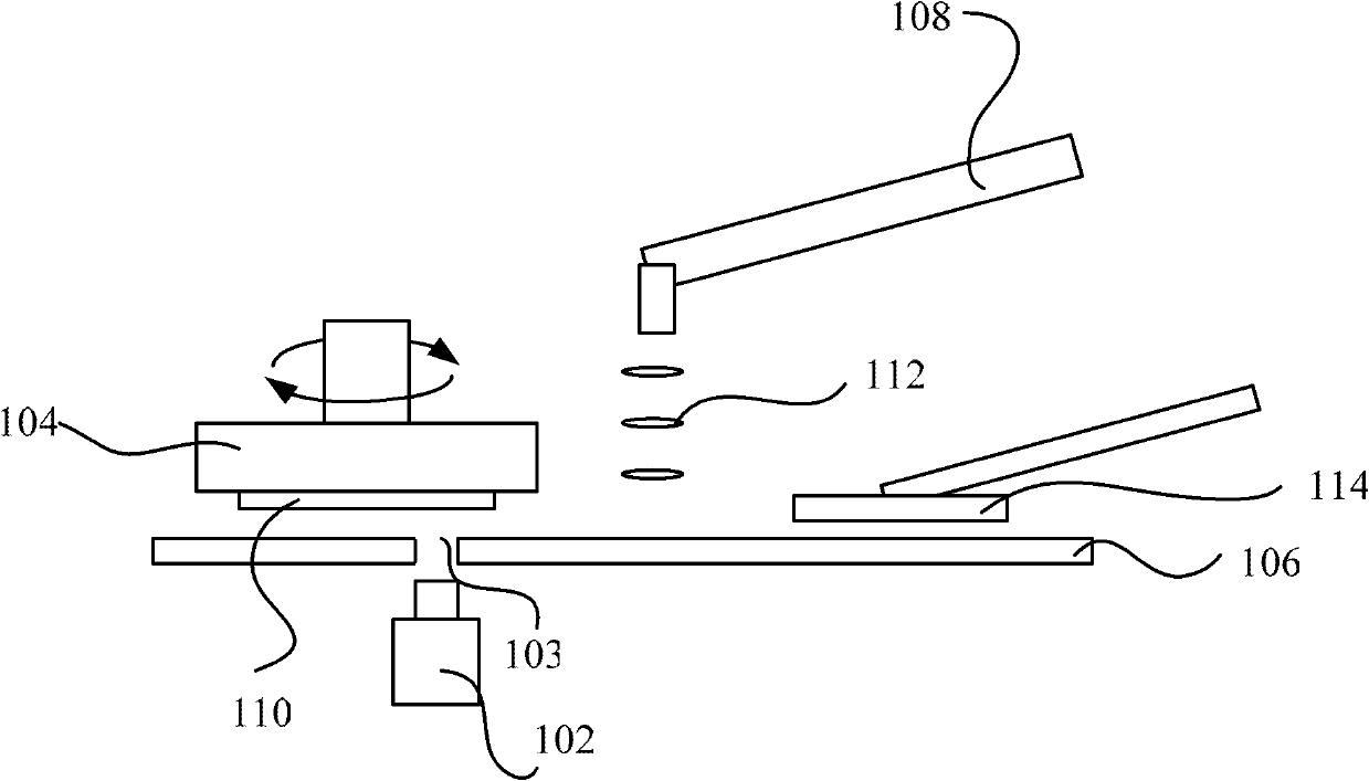
[0009] However, the position of the laser in the existing optical endpoint detection method is fixed, and the wafer surface can only be scanned step by step during the rotation of the wafer. There will be a delay in time, and the time required to scan the entire wafer will increase with the increase in the number of wafers. increases with increasing circle size, so as the wafer size increases, the impact of this time delay becomes greater and greater
In addition, the light transmittance of the light-transmitting area also has a great influence on the measurement results, and due to the limitation of the light transmittance of the light-transmitting area, the detection error is relatively large

Method used


Image

  • Chemical mechanical grinding device
  • Chemical mechanical grinding device
  • Chemical mechanical grinding device

Examples


Embodiment Construction

[0035] It can be seen from the background technology that the existing chemical mechanical polishing device has a time delay when detecting the grinding, and as the wafer size increases, the impact caused by the delay becomes more and more obvious; in addition, in order to adopt the existing grinding detection When the device performs grinding detection, a transparent area must be formed on the polishing pad. Because the incident light is incident on the wafer surface through the transparent area, the position and light transmittance of the transparent area have a great influence on the detection accuracy, so it is easy to cause The light transmittance of the projection area is not uniform or the light transmittance is not high enough to affect the detection accuracy. The inventors of the present invention conducted research on the above problems, and provided a chemical mechanical polishing device in the present invention.

[0036] The chemical mechanical polishing device pro...


PUM


Abstract

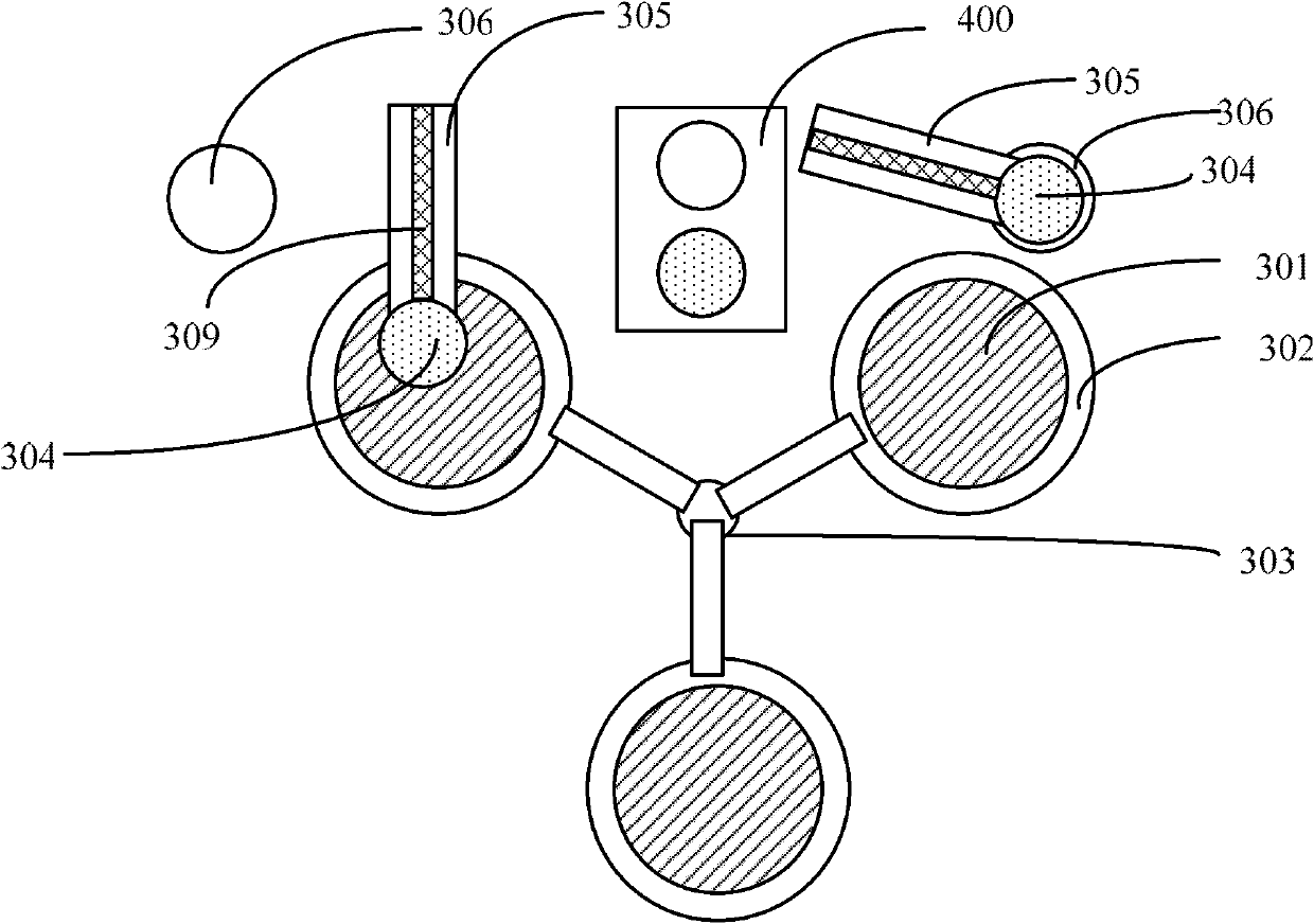
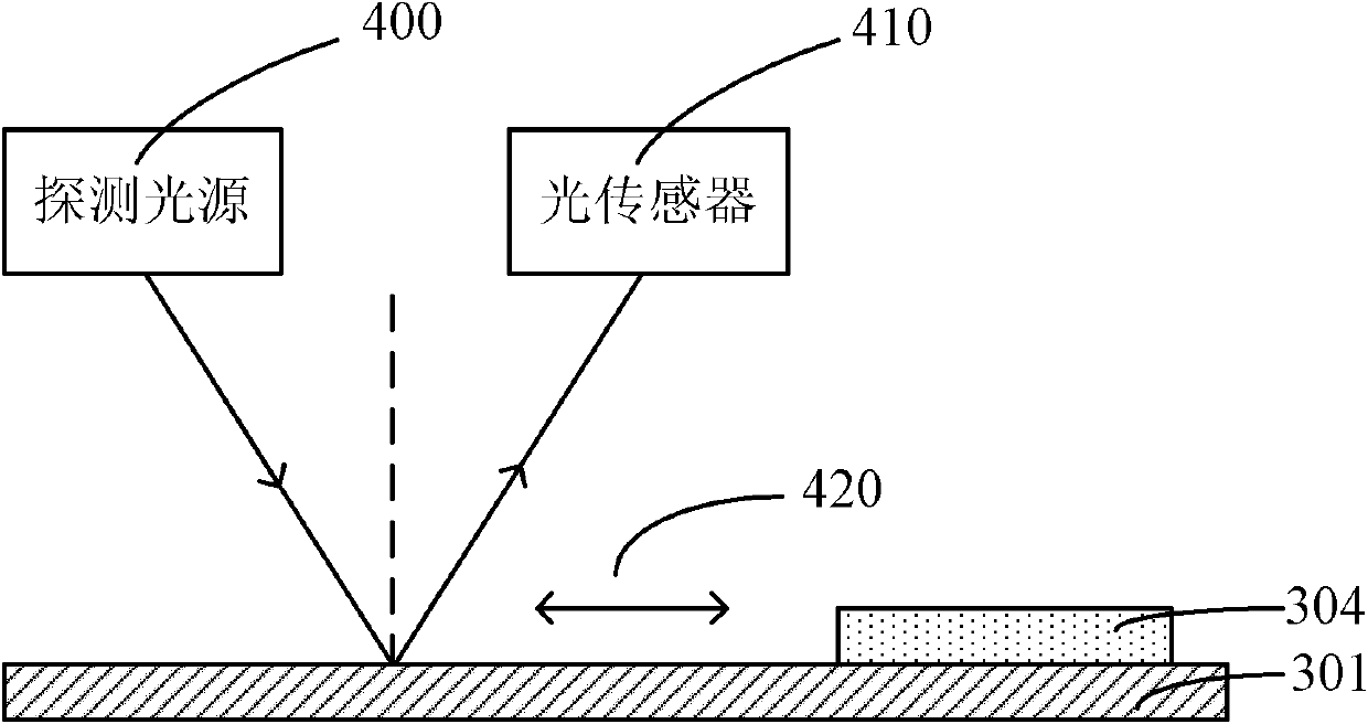
A chemical mechanical grinding device comprises a grinding disc, a grinding pad arm, a grinding pad, a grinding pulp supply route and a grinding detection device. The grinding disc is used for bearing supplied wafers. One end of the grinding pad is fixed. The grinding pad is fixed at the non-fixed end of the grinding pad arm and is capable of being in motion relative to the supplied wafers when driven by the grinding pad arm, the grinding pad arm determines a motion period, the grinding pad is contacted with the supplied wafers. Grinding pulp is supplied by the grinding pulp supply route between the grinding pad and the grinded wafers during the grinding period. The grinding detection device synchronously detects the grinding state of entire wafers. By means of the chemical mechanical grinding device, synchronism of grinding detection can be improved.

Description

technical field [0001] The invention relates to the field of semiconductors, in particular to a chemical mechanical grinding device. Background technique [0002] The chemical mechanical polishing (CMP, Chemical Mechanical Polishing) process was introduced into the integrated circuit manufacturing industry by IBM in 1984, and was first used for the planarization of the intermetal dielectric (IMD, Inter Metal Dielectric) in the subsequent process, and then through equipment and processes The modification was used for planarization of tungsten, followed by shallow trench isolation (STI) and copper planarization processes. Chemical mechanical polishing is a very active technology in IC manufacturing process in recent years. [0003] The mechanism of chemical mechanical polishing is that the surface material of the wafer to be ground reacts chemically with the slurry to generate a relatively easy-to-remove surface layer, which is passed through the abrasive in the slurry and th...

Claims


Application Information

Patent Timeline
Patent Type & Authority Applications(China)
IPC IPC(8): B24B37/00B24B37/005B24B37/20B24B57/02H01L21/304
Inventor 蒋莉黎铭琦
Owner SEMICON MFG INT (SHANGHAI) CORP
Learn More