
Silicon PIN neutron dose detector and manufacture method thereof

A neutron dose and detector technology, which is applied in the field of silicon PIN neutron dose detectors and its preparation, can solve the problems of increased production cost and process difficulty, silicon PIN detector defects, etc., and achieve cost reduction and process complexity, Reduced requirements, effects of uniform current distribution

Inactive Publication Date: 2012-07-04
PEKING UNIV
View PDF3 Cites 2 Cited by
  • Summary
  • Abstract
  • Description
  • Claims
  • Application Information

AI Technical Summary

Problems solved by technology

[0005] Although silicon PIN detectors have the advantages described above, the above-mentioned silicon PIN detectors also have drawbacks
Published experimental research results show that the sensitivity of neutron detection depends on the distance between the P region and the N region, that is, the thickness of the I region, which requires a larger thickness of the silicon substrate, so that the above silicon neutron dose detection The sensitivity of the device is limited by the thickness of the silicon substrate, while increasing the production cost and process difficulty

Method used


Image

  • Silicon PIN neutron dose detector and manufacture method thereof
  • Silicon PIN neutron dose detector and manufacture method thereof
  • Silicon PIN neutron dose detector and manufacture method thereof

Examples


Embodiment Construction

[0034] The present invention will be further described through specific embodiments below in conjunction with the accompanying drawings, but the scope of the present invention is not limited in any way.

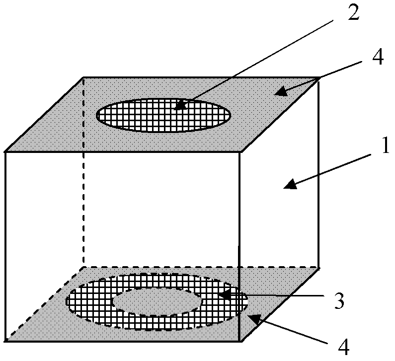
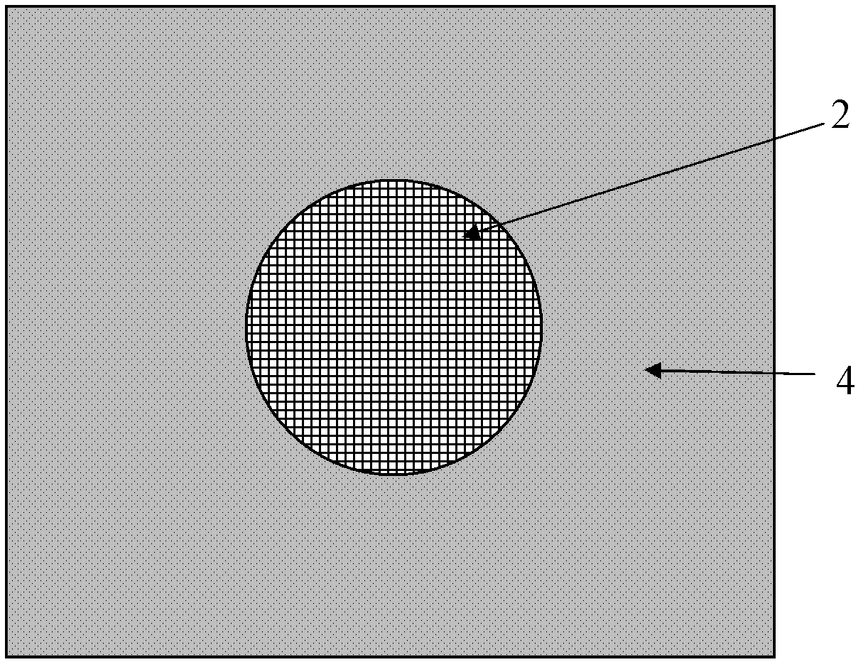
[0035] The following examples are intended to be prepared by a specific manufacturing method figure 2 The silicon PIN neutron dose detector shown, the silicon PIN neutron dose detector includes a double-sided polished high-resistance silicon wafer 1 as a substrate, and has a circular P-type active layer on the front and back sides of the silicon wafer 1 Area 2 and N-type active area 3, silicon dioxide layer 4 is on the silicon surface outside the active area.

[0036] Concrete manufacturing method comprises the following steps:

[0037] 1. If Pic 4-1 As shown, a double-sided polished high-resistance silicon wafer 1 as a substrate is oxidized at a high temperature of 1000 ° C, and a thickness of 8000 is formed on the upper and lower surfaces of the silicon wafer. the sil...


PUM

PropertyMeasurementUnit
Thicknessaaaaaaaaaa
Diameteraaaaaaaaaa

Abstract

The invention discloses a silicon PIN neutron dose detector and a manufacture method thereof. The silicon PIN neutron dose detector comprises a high-resistance silicon chip, as well as a P type active area and an N type active area, which are respectively positioned on the front surface and the back surface of the silicon chip, wherein one of the active areas is circular, and the other active area is annular. According to the silicon PIN neutron dose detector disclosed by the invention, the P type active area and the N type active area are designed into of an upper and down asymmetric structure, so that the distance between the P area and the N area is greater than the thickness of the silicon chip, the distance between the two active areas is effectively increased, namely the effective thickness of an I region of the detector is increased, and the restriction of the thickness of the silicon chip on the thickness of the I region of a PIN tube is also broken through. In addition, the annular active area can generate more uniform current distribution through the symmetry of the structure of the annular active area.

Description

technical field [0001] The invention relates to a silicon PIN neutron dose detector used in neutron dose detection, in particular to a silicon PIN neutron dose detector used in nuclear detection with higher performance requirements and a preparation method thereof. Background technique [0002] Neutron dose detection is the use of fast neutrons to irradiate silicon materials to cause defects inside the silicon lattice. The lattice defects will act as effective recombination centers to reduce the lifetime of minority carriers, thereby changing the voltage and current characteristics of silicon devices. Detect changes in the voltage and current characteristics of silicon devices to reflect the total dose of neutron radiation it receives over a period of time. [0003] Since the 1960s, silicon PIN detectors have been developed and applied to nuclear physics detection. The basic structure of the silicon PIN neutron dose detector is as follows: figure 1 As shown, a high-resista...

Claims


Application Information

Patent Timeline
IPC IPC(8): H01L31/118H01L31/18G01T3/00
CPCY02P70/50
Inventor 樊超于民杨昉东田大宇王金延金玉丰
Owner PEKING UNIV
Learn More