Eureka AIR delivers breakthrough ideas for toughest innovation challenges, trusted by R&D personnel around the world.

Alignment marking method in DMOS (Double-diffusion Metal Oxide Semiconductor) process flow

A technology of alignment marking and process flow, applied in the manufacture of electrical components, electrical solid devices, semiconductor/solid devices, etc., can solve problems such as temperature must be increased, production line equipment program configuration is complicated, and the surface of the wafer is rough, etc., to ensure normal counterpoint effect

Active Publication Date: 2012-07-04
CSMC TECH FAB2 CO LTD
View PDF7 Cites 3 Cited by
  • Summary
  • Abstract
  • Description
  • Claims
  • Application Information

AI Technical Summary

Problems solved by technology

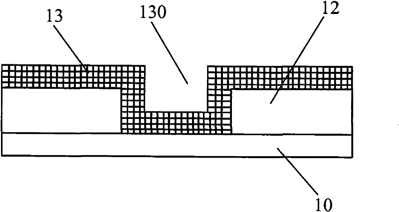
like Figure 5 As shown, the thick aluminum deposition will be carried out at last, because the thick aluminum lithography uses the second alignment mark hole 130 in the alignment mark hole 120, after the mark hole undergoes chemical mechanical polishing and thick aluminum deposition, the step mark Extremely shallow, resulting in a weak alignment mark signal, leading to various alignment problems, and sometimes even requiring manual assistance from production line operators. When the manual operation fails, the product can only be scrapped
[0006] A kind of improved method is to cancel the tungsten deposition, and directly deposit aluminum in the alignment mark hole 120, although the step of the alignment mark becomes larger, the following problems will be produced thereupon: 1. The temperature of aluminum deposition must be 2. When aluminum is deposited at high temperature, it is easy to produce larger grains, resulting in rough surface of the wafer, which will also affect the alignment effect

Method used

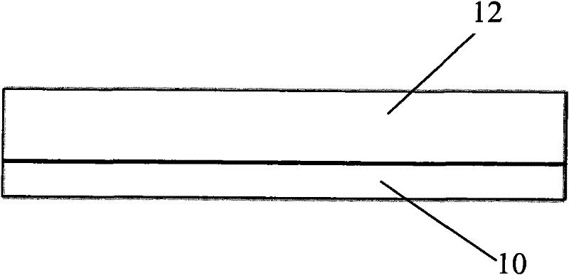
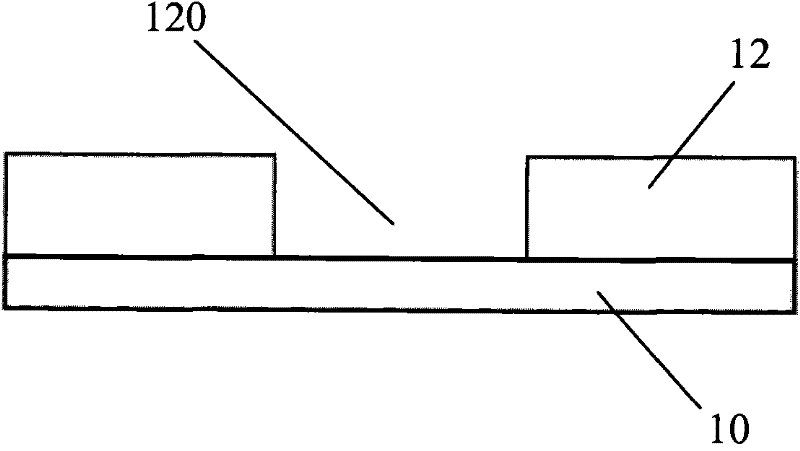

Image

  • Alignment marking method in DMOS (Double-diffusion Metal Oxide Semiconductor) process flow
  • Alignment marking method in DMOS (Double-diffusion Metal Oxide Semiconductor) process flow
  • Alignment marking method in DMOS (Double-diffusion Metal Oxide Semiconductor) process flow

Examples


Embodiment Construction

[0019] The implementation process and essential content of the present invention will be described below with preferred embodiments with reference to the accompanying drawings.

[0020] Such as Image 6 As shown, there is an inorganic membrane structure 101 above the wafer base 100, and the inorganic membrane structure 101 forms a groove 102 after groove etching, and the groove 102 is the most important and basic first alignment for other subsequent processes. mark. The first alignment mark 102 must be concave, and the width must be large enough, otherwise it is easy to be filled with polysilicon and tungsten in the subsequent process engineering. After considering the filling factor, the mark width of the first alignment mark 102 is generally designed to be 4-6 microns.

[0021] Such as Figure 7 with Figure 8 As shown, after the trench 102 is formed, the polysilicon 200 filling begins to form the trench gate. The polysilicon 200 begins to fill both sides of the trench ...


PUM

PropertyMeasurementUnit
Widthaaaaaaaaaa
Thicknessaaaaaaaaaa
Thicknessaaaaaaaaaa

Abstract

The invention discloses an alignment marking method which comprises the steps of: providing a wafer substrate provided with an inorganic film structure, carrying out groove etching on the inorganic film structure to form a groove and first alignment marks; carrying out polysilicon filling by depending on the first alignment marks, covering the organic film structure and filling partial groove by polysilicon, then removing partial polysilicon in the groove through photoetching and forming second alignment marks; carrying out hole medium filling by depending on the second alignment marks, filling a hole medium layer in the second alignment marks and covering the upper surface of the polysilicon, then removing partial hole medium between the second alignment marks through etching to form third alignment marks; carrying out tungsten deposition by depending on the third alignment marks, covering the upper surface of the hole medium layer and filling partial third alignment marks by tungsten to form fourth alignment marks, then removing tungsten on the surface of the hole medium layer by adopting a chemical mechanical polishing manner; and carrying out aluminum deposition by depending on the fourth alignment marks, and filling the fourth alignment marks and covering the upper surface of the hole medium layer by aluminum.

Description

technical field [0001] The invention relates to the field of manufacturing semiconductor devices, in particular to a method for manufacturing a trench type DMOS transistor. Background technique [0002] A DMOS (Double Diffused MOS) transistor is a type of MOSFET (Metal Field Effect Transistor on Semiconductor) that uses diffusion to form the transistor region. DMDS transistors are generally used as power transistors to provide high voltage circuits for power integrated circuit applications. DMOS transistors provide higher current per unit area when low forward voltage drop is required. [0003] A specific type of DMOS transistor is the trench DMOS transistor, in which the channel occurs on the inner walls of the trench extending from the source to the drain, and the gate is formed within the trench. Therefore, trench DMOS transistors have the characteristics of high current drive capability, low on-resistance and high breakdown voltage, and are widely used in computer moth...

Claims


Application Information

Patent Timeline
IPC IPC(8): H01L21/336H01L21/02H01L21/3205H01L23/544
CPCH01L2924/0002
Inventor 黄玮
Owner CSMC TECH FAB2 CO LTD
Why Eureka
Eureka Blog
Learn More