Method for raising signal to noise ratio of piezoelectric electret film sensor
A piezoelectric electret and thin-film sensor technology, applied in the manufacture/assembly of piezoelectric/electrostrictive devices, piezoelectric/electrostrictive/magnetostrictive devices, circuits, etc., can solve complex processes and signal distortion , restricted use and other issues, to achieve the effect of improving signal-to-noise ratio, reducing noise interference, and improving work efficiency
- Summary
- Abstract
- Description
- Claims
- Application Information
AI Technical Summary
Problems solved by technology
Method used
Image
Examples
Embodiment example 1
[0035] Implementation Case 1 [as attached figure 1 ]
[0036] Commercially available conductive double-sided adhesive tape was laminated on the positive electrode surface of the prepared piezoelectric electret film 1 coated with metal electrodes. The piezoelectric electret film 1 with the conductive glue attached to the positive electrode surface is laminated on the commercially available negative electrode surface coated with a metal electrode piezoelectric electret film 2, and the piezoelectric electret film 1 and piezoelectric The electret film 2 sticks together. Then commercially available plastic films 3 and 4 were cold mounted on the negative electrode surface of the piezoelectric electret film 1 and the positive electrode surface of the piezoelectric electret film 2 respectively. The commercially available conductive ink 5 is screen-printed on the outer surface of the plastic film 3 of the piezoelectric electret film assembly, and then the above-mentioned assembly is ...
Embodiment example 2
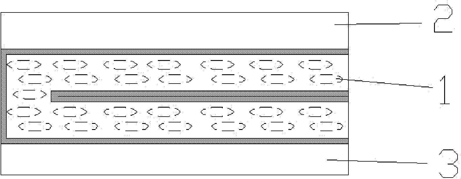
[0038] Implementation case two [as attached figure 2 ]
[0039] Commercially available conductive double-sided adhesive tape was laminated on the positive electrode surface of the prepared piezoelectric electret film 1 coated with metal electrodes. Fold the commercially available piezoelectric electret film 1 with conductive glue on the positive electrode surface into the positive electrode surface and then laminate it. Then commercially available plastic films 2 and 3 were cold-mounted on the upper and lower negative electrode surfaces of the above-mentioned piezoelectric electret film 1 assembly, respectively. The metal terminals are drawn out to complete the piezoelectric electret film parallel self-shielding laminated sensor.
[0040] A schematic diagram of the comparison of output charges between the parallel stacked sensor 1 and the single-layer sensor 2 is shown in FIG. 5 .
Embodiment example 3
[0041] Implementation case three [as attached image 3 ]
[0042] The commercially available plastic films 2 and 3 are cold mounted on the positive and negative electrode surfaces of the commercially available piezoelectric electret film 1, respectively. The commercially available conductive ink 4 is screen-printed on the outer surface of the plastic film 2 of the piezoelectric electret film assembly, and then the above assembly is placed in an oven for 30 minutes at 100 degrees Celsius and then taken out. Finally, a commercially available plastic film 5 is cold mounted on the upper surface of the conductive ink 4 of the piezoelectric electret film assembly. The metal terminals are drawn out to complete the piezoelectric electret film series and shielded laminated sensor.
[0043] The output schematic diagram of the above-mentioned single-layer sensor with shielding layer is shown in Figure 6;
[0044] The schematic diagram of the output of the single-layer sensor 2 without...
PUM
 Abstract
Description
Claims
Application Information
 - R&D
- Intellectual Property
- Life Sciences
- Materials
- Tech Scout
- Unparalleled Data Quality
- Higher Quality Content
- 60% Fewer Hallucinations
Browse by: Latest US Patents, China's latest patents, Technical Efficacy Thesaurus, Application Domain, Technology Topic, Popular Technical Reports.
© 2025 PatSnap. All rights reserved.Legal|Privacy policy|Modern Slavery Act Transparency Statement|Sitemap|About US| Contact US: help@patsnap.com


