
Pixel structure, active element array substrate and planar display panel

A technology of pixel structure and active components, which is applied in the direction of electrical components, electric solid devices, semiconductor devices, etc., can solve the problems of reducing the available area of ​​storage capacitors, failing to increase storage capacitors, and changes in parasitic capacitance values, so as to improve the quality of screen display, Reduce asymmetrical gate-drain capacitance and increase the effect of storage capacitance

Active Publication Date: 2012-04-04
AU OPTRONICS CORP
View PDF4 Cites 22 Cited by
  • Summary
  • Abstract
  • Description
  • Claims
  • Application Information

AI Technical Summary

Problems solved by technology

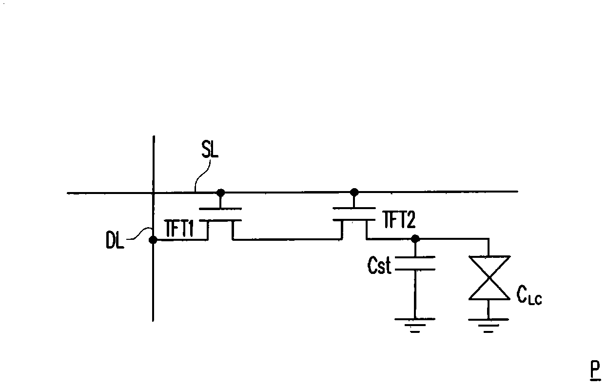
However, in order to maintain the electrical performance of the pixel structure P (such as reducing the leakage current and increasing the conduction current), a layout design in which two thin film transistors are connected in series must be adopted, and the additional thin film transistors will reduce the available area of ​​the storage capacitor (Cst). , but cannot increase the storage capacitance (Cst)
On the other hand, if the layout area of ​​the first thin film transistor TFT1 and the second thin film transistor TFT2 is reduced and the layout area of ​​the common electrode is increased in order to increase the storage capacitance (Cst), the electrical properties of the element will be affected.
For example, the process offset between the gate and the source and the drain causes a change in the parasitic capacitance (parasitic capacitance), causing the display screen to flicker

Method used


Image

  • Pixel structure, active element array substrate and planar display panel
  • Pixel structure, active element array substrate and planar display panel
  • Pixel structure, active element array substrate and planar display panel

Examples


Embodiment Construction

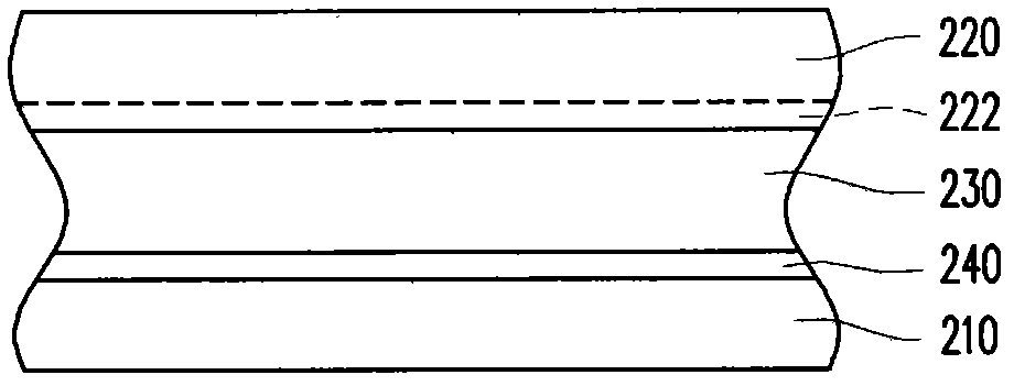
[0061] figure 2 is a schematic cross-sectional view of a flat display panel according to an embodiment of the present invention. Please refer to figure 2 , the flat display panel includes a first substrate 210 , a second substrate 220 , a display medium 230 and an active device array 240 . The second substrate 220 is disposed above the first substrate 210 . The second substrate 220 may be a simple blank substrate or a substrate further including the opposite electrode 222 . The display medium 230 is disposed between the first substrate 210 and the second substrate 220 . The display medium 230 is, for example, an electrophoretic display film, an organic electroluminescence layer or a liquid crystal layer, wherein the electrophoretic display film can be a microcapsule electrophoretic display film or a microcup electrophoretic display film, which is known to those skilled in the art are well known, so no further details are given. The active device array 240 is disposed on...


PUM


Abstract

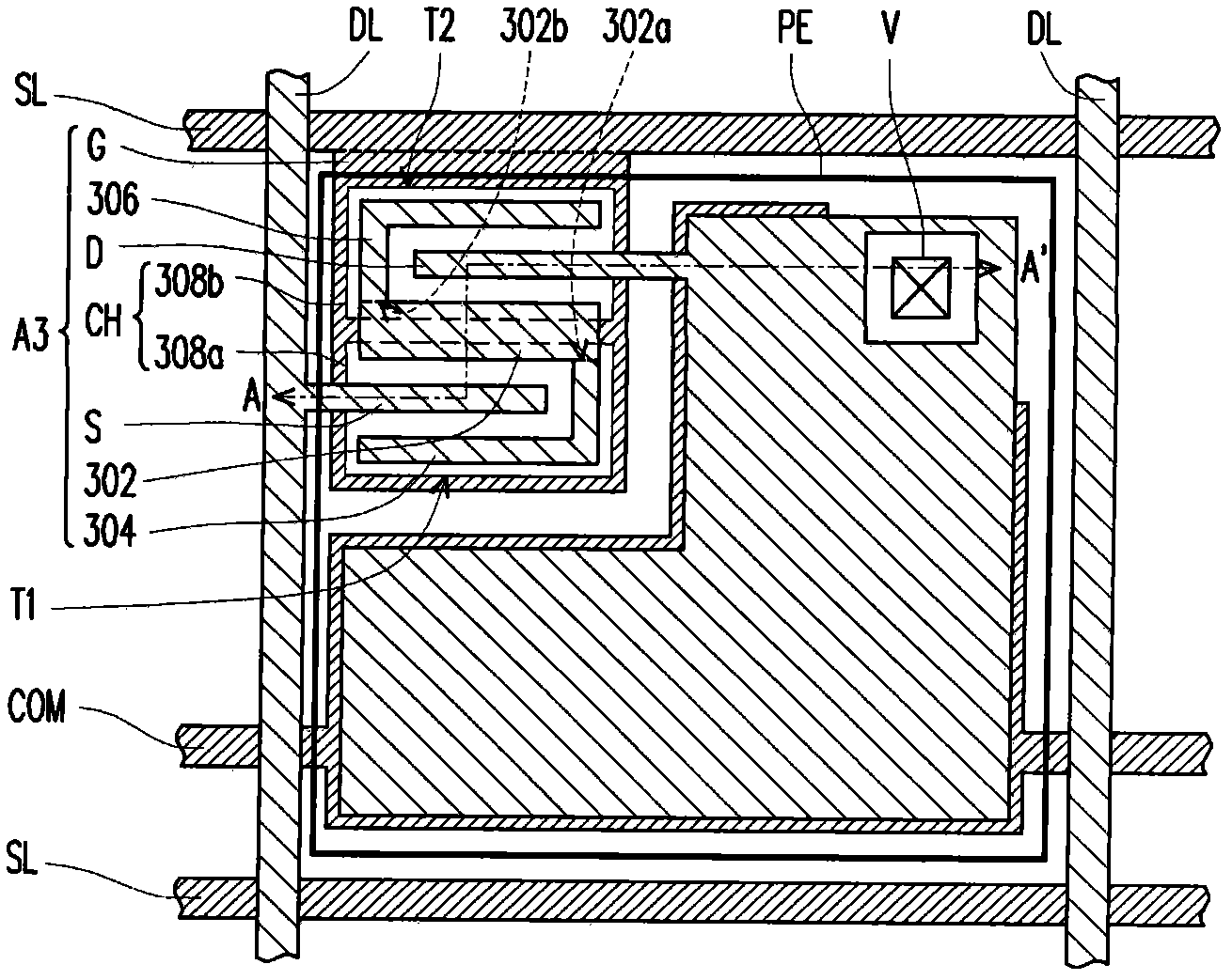
The invention discloses a pixel structure, an active element array substrate and a planar display panel. The pixel structure comprises a pixel electrode and an active element. The active element comprises a grid electrode, a channel layer, a source electrode, a drain electrode, a connecting electrode, a first branch part and a second branch part. The grid electrode is electrically connected with a scanning line. The channel layer is located on one side of the grid electrode and electrically insulated from the grid electrode. The source electrode and the data line are electrically connected. The drain electrode and the pixel electrode are electrically connected. The source electrode, the drain electrode and the connecting electrode are equipped on parts of the channel layer. The connecting electrode is located between the source electrode and the drain electrode. The first branch part is equipped on the parts of the channel layer and connected with one end of the connecting electrode. The first branch part surrounds the source electrode located on the channel layer. The second branch part is equipped on parts of the channel layer and connected with the other end of the connecting electrode. The second branch part surrounds the drain electrode located on the channel layer.

Description

technical field [0001] The invention relates to a pixel structure, an active element array substrate and a flat display panel with the pixel structure. Background technique [0002] With the advancement of display technology, people can make their lives more convenient with the assistance of displays. In order to achieve the characteristics of lightness and thinness of displays, flat panel displays (FPDs) have become the current mainstream. Generally speaking, a pixel structure in a flat panel display includes an active element and a pixel electrode, wherein the active element is used as a switch element of a display unit. In order to control a specific pixel structure, a specific pixel is usually selected through a corresponding scan line and a data line, and an appropriate operating voltage is provided to display display data corresponding to the pixel. In addition, the pixel structure also includes a storage capacitor to store the above-mentioned applied operating voltag...

Claims


Application Information

Patent Timeline
Patent Type & Authority Applications(China)
IPC IPC(8): G02F1/1362G02F1/1368G02F1/1343G02F1/167
CPCG02F1/1368G02F1/1362G02F1/13624G02F1/1343G02F1/167H01L27/124H01L29/41733
Inventor 魏全生江明道林昱廷陈茂松黄伟明
Owner AU OPTRONICS CORP
Learn More