
Techniques for non-overlapping clock generation

A clock generation circuit, non-overlapping technology, applied in the direction of pulse technology, pulse generation, generation of electrical pulses, etc., can solve the problems of consuming the effective time of the clock, multi-current, consumption, etc.

Inactive Publication Date: 2012-03-07
QUALCOMM INC
View PDF8 Cites 16 Cited by
  • Summary
  • Abstract
  • Description
  • Claims
  • Application Information

AI Technical Summary

Problems solved by technology

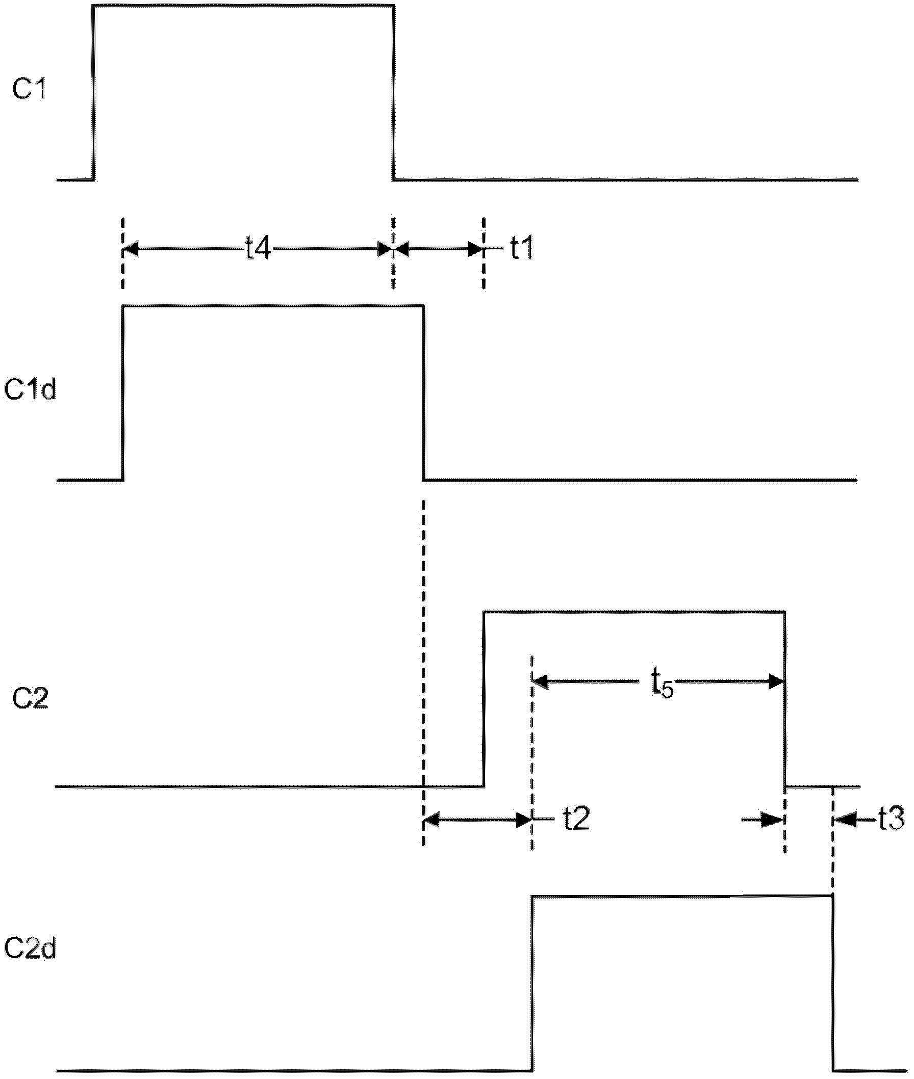
The extra non-overlap time and phase delay time in slow corner conditions consumes the active time of the clock and requires faster stabilization of the switched capacitor integrator
Therefore, more current is consumed for the op-transconductance amplifier in the switched capacitor integrator
Also, as the switched capacitor integrator sampling frequency (fs) increases, the non-overlap time and phase delay become more significant relative to the active time of the clock signal

Method used


Image

  • Techniques for non-overlapping clock generation
  • Techniques for non-overlapping clock generation
  • Techniques for non-overlapping clock generation

Examples


Embodiment Construction

[0021] The word "exemplary" is used herein to mean "serving as an example, illustration, or illustration." Any embodiment or design described herein as "exemplary" is not to be construed as preferred or advantageous over other embodiments or designs.

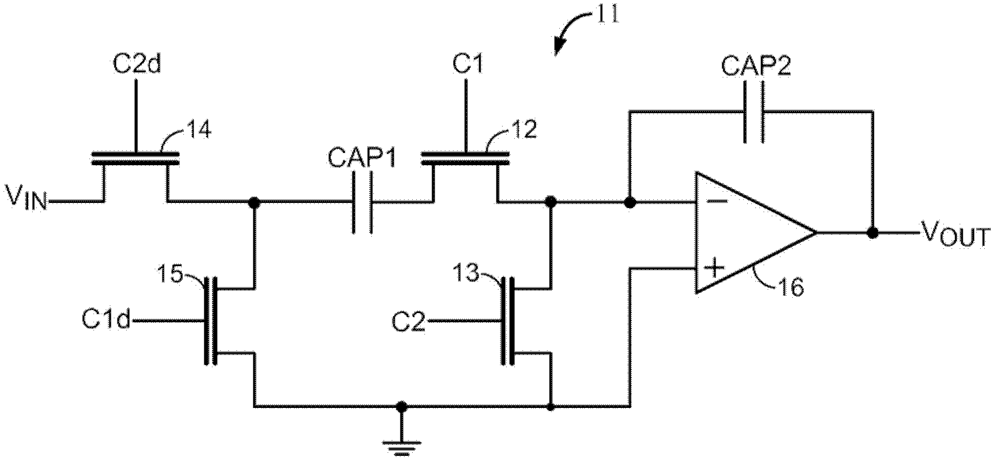
[0022] Typically, non-overlapping clock signals are used in switched capacitor circuits to minimize errors. FIG. 1 is a schematic diagram of a prior art non-inverting switched capacitor integrator circuit 11 known to those skilled in the art. The switched capacitor integrator circuit 11 includes switches 12 , 13 , 14 and 15 , capacitors CAP1 and CAP2 , and an amplifier 16 . Switches 12, 13, 14 and 15 receive non-overlapping clock signals C1, C2, C2d (C2-delay) and C1d (C1-delay), respectively.

[0023] In a first phase of operation, switches 13 and 14 are enabled to charge capacitor CAP1 to a voltage applied to input Vin. A switch 14 connects the input Vin to the first terminal of the capacitor CAP1. Switch 13 connects the s...


PUM


Abstract

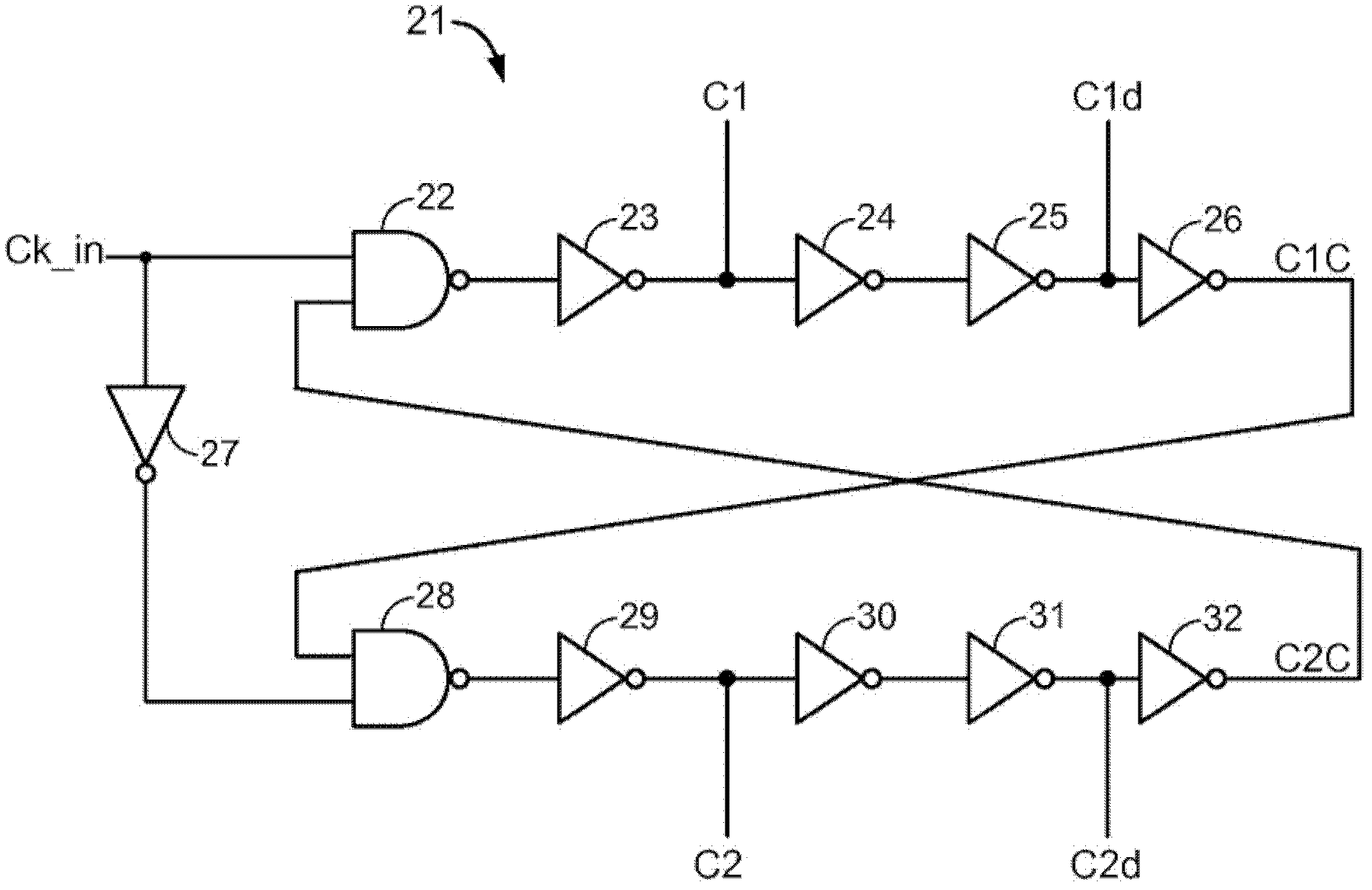
Techniques for generating precise non-overlap time and clock phase delay time across a desired frequency range are provided. In one configuration, a device includes a non-overlapping clock generation circuit which comprises a delay lock loop (DLL) circuit that in turn generates a control voltage to a clock generator circuit coupled thereto. The control voltage operates to maintain precise timing relationship of non- overlapping delayed clock signals generated by the clock generator circuit. In one aspect, the DLL circuit receives an input clock with a known duty cycle and derives an output control voltage to fix the unit delay to a certain portion of the input clock cycle. In a further aspect, the clock generator circuit includes a plurality of voltage-controlled delay cells coupled to the DLL circuit to generate a first set of clock signals and a second set of clock signals delayed from the first set of clock signals by a non- overlapping time (tnlp) that is independent of manufacturing process variations.

Description

technical field [0001] The present invention relates generally to the field of clock generation circuits, and in particular, to non-overlapping clock generation circuits. Background technique [0002] Typically, clock generation circuits are used to clock synchronous digital circuits such as analog-to-digital converters (ADCs). A clock generation circuit provides a repetitive signal with a constant period. During a single clock signal period, the clock signal has a first phase and a second phase. Typically, a clock generation circuit provides an inverted clock signal and a non-inverted clock signal. The clock generation circuit also typically provides a delayed clock signal. [0003] One type of clock signal is a non-overlapping clock signal. Non-overlapping clock signals are often used in switched capacitor integrator circuits. The non-overlapping clock generation circuit provides a non-inverted clock signal and an inverted clock signal that transitions before the dela...

Claims


Application Information

Patent Timeline
Patent Type & Authority Applications(China)
IPC IPC(8): H03L7/08H03K3/017H03M1/12
CPCH03K5/1515H03K5/1565H03K2005/00039H03K2005/00097H03K2005/00286H03L7/0812H03M1/12H03K3/017H03L7/08
Inventor X·全T·宋L·马特D·J·阿拉蒂
Owner QUALCOMM INC
Learn More