
AMOLED (Active Matrix/Organic Light-Emitting Diode) pixel circuit and driving method thereof

A technology of pixel circuits and row pixels, which is applied in instruments, static indicators, etc., can solve the problems of inconsistent organic light-emitting diode OLED, inconsistent brightness of organic light-emitting diode OLED, and deterioration of display image quality, so as to improve response characteristics and uniform image quality Effect

Active Publication Date: 2012-02-08
KUNSHAN NEW FLAT PANEL DISPLAY TECH CENT
View PDF4 Cites 57 Cited by
  • Summary
  • Abstract
  • Description
  • Claims
  • Application Information

AI Technical Summary

Problems solved by technology

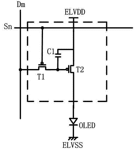
However, in such a conventional active matrix organic light emitting diode display device, it is difficult to display an image with uniform brightness due to the threshold voltage variation of the second transistor T2 and the leakage current of the first transistor T1
[0014] For example, due to the differences in the threshold voltages of the second transistor T2 in different pixels, the current flowing through the organic light emitting diode OLED is inconsistent when the same gate driving voltage is applied, resulting in inconsistent brightness of the organic light emitting diode OLED, and each pixel responds The same data signal produces light with different brightness, making it difficult to display an image with uniform brightness
[0015] Another example is that the gate voltage of the second transistor T2 changes due to the leakage current of the first transistor T1, causing the current flowing through the organic light emitting diode OLED to change, causing the brightness of the organic light emitting diode OLED to change during the light-emitting time period, resulting in deterioration of display image quality

Method used


Image

  • AMOLED (Active Matrix/Organic Light-Emitting Diode) pixel circuit and driving method thereof
  • AMOLED (Active Matrix/Organic Light-Emitting Diode) pixel circuit and driving method thereof
  • AMOLED (Active Matrix/Organic Light-Emitting Diode) pixel circuit and driving method thereof

Examples


Embodiment Construction

[0037] The present invention will be further described below in conjunction with the accompanying drawings and embodiments.

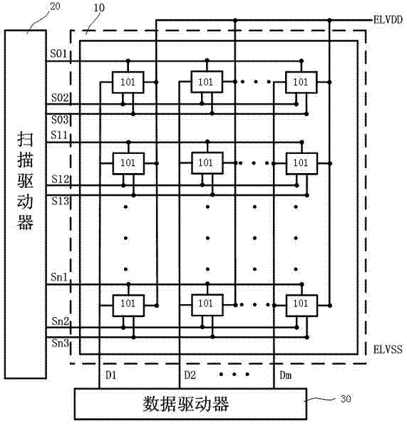
[0038] figure 2 It is a schematic structural diagram of the active matrix organic light emitting display device of the present invention.

[0039] See figure 2 , the active matrix organic light-emitting display device of the present invention includes: a display unit 10, a scan driver 20 and a data driver 30; the display unit 10 includes a plurality of pixels 101, and the plurality of pixels 101 are arranged in a matrix on the scan control line Sn1, Sn2 and Sn3, and the intersection area of ​​the data lines D1 to Dm.

[0040] Each pixel 101 is connected to a scan control line (for example, Sn1 , Sn2 and Sn3 ) and a data line (the data line is connected to the column of pixels 101 in which the pixel 101 itself is located). For example, the pixel 101 located in the i-th row and the j-th column is connected to the i-th scanning control lines Si1, Si2 an...


PUM


Abstract

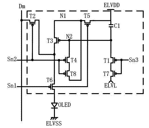
The invention discloses an AMOLED (Active Matrix / Organic Light-Emitting Diode) pixel circuit and a driving method thereof. The AMOLED pixel circuit comprises pixel units which are distributed in an n-row, m-column matrix, the pixel units are connected with a data driver through data lines and a scanning driver through scanning lines, each pixel unit comprises an organic light-emitting diode (OLED), and n and m are natural numbers; each row pixel unit comprises a first scanning control line Sn1, a second scanning control line Sn2 and a third scanning control line Sn3; the OLED is connected between the drain of a sixth transistor T6 and a second power supply ELVSS; and each row pixel unit also comprises threshold voltage compensation transistors T4 and T8 and leakage current compensation transistors T1 and T7. By arranging the threshold voltage compensation transistors and the leakage current compensation transistors, the response characteristic of the active matrix OLED is improved, and thereby images with uniform image quality can be displayed.

Description

technical field [0001] The present invention relates to a pixel circuit and its driving method, in particular to an AMOLED pixel circuit and its driving method. Background technique [0002] In recent years, various types of flat panel display devices that are lighter in weight and smaller in size than cathode ray tubes have been developed. [0003] Among various types of flat-panel display devices, active matrix organic light-emitting display devices use self-luminous organic light-emitting diodes (OLEDs) to display images, usually have a short response time, use low power consumption for driving, and relatively better brightness and color purity characteristics, so organic light emitting display devices have become the focus of next generation display devices. Organic light-emitting diodes can be driven by passive matrix (PM) or active matrix (AM). Compared with the PM drive, the AM drive has the advantages of larger displayed information capacity, lower power consumpti...

Claims


Application Information

Patent Timeline
Patent Type & Authority Applications(China)
IPC IPC(8): G09G3/32G09G3/3233G09G3/3258
Inventor 朱晖邱勇罗红磊高孝裕
Owner KUNSHAN NEW FLAT PANEL DISPLAY TECH CENT
Learn More