
Method for manufacturing gallium nitride compound semiconductor, and semiconductor light emitting element

A manufacturing method, gallium nitride-based technology, applied in semiconductor/solid-state device manufacturing, semiconductor devices, chemical instruments and methods, etc., can solve the unrealistic characteristics of light-emitting elements, m-plane InGaN layer crystal defects and increased holes, Problems such as decreased crystallinity of the m-plane InGaN layer

Inactive Publication Date: 2012-01-11
PANASONIC CORP
View PDF4 Cites 2 Cited by
  • Summary
  • Abstract
  • Description
  • Claims
  • Application Information

AI Technical Summary

Problems solved by technology

In this way, if the growth temperature is lowered to a temperature close to 700°C, the obtained m-plane InGaN layer will have more crystal defects and holes, and the crystallinity of the m-plane InGaN layer will be significantly reduced.
In addition, the reduction of the growth temperature also becomes the NH in the reaction chamber 3 The reason for the reduction of the decomposition efficiency
Therefore, m-plane growth at an extremely low temperature of less than 700°C is also unrealistic in terms of the characteristics of light-emitting devices.

Method used


Image

  • Method for manufacturing gallium nitride compound semiconductor, and semiconductor light emitting element
  • Method for manufacturing gallium nitride compound semiconductor, and semiconductor light emitting element
  • Method for manufacturing gallium nitride compound semiconductor, and semiconductor light emitting element

Examples


Embodiment approach

[0134] As follows, while referring to Figure 14 , while describing an embodiment in which a semiconductor light-emitting element is manufactured according to the method for manufacturing a gallium nitride-based compound semiconductor of the present invention.

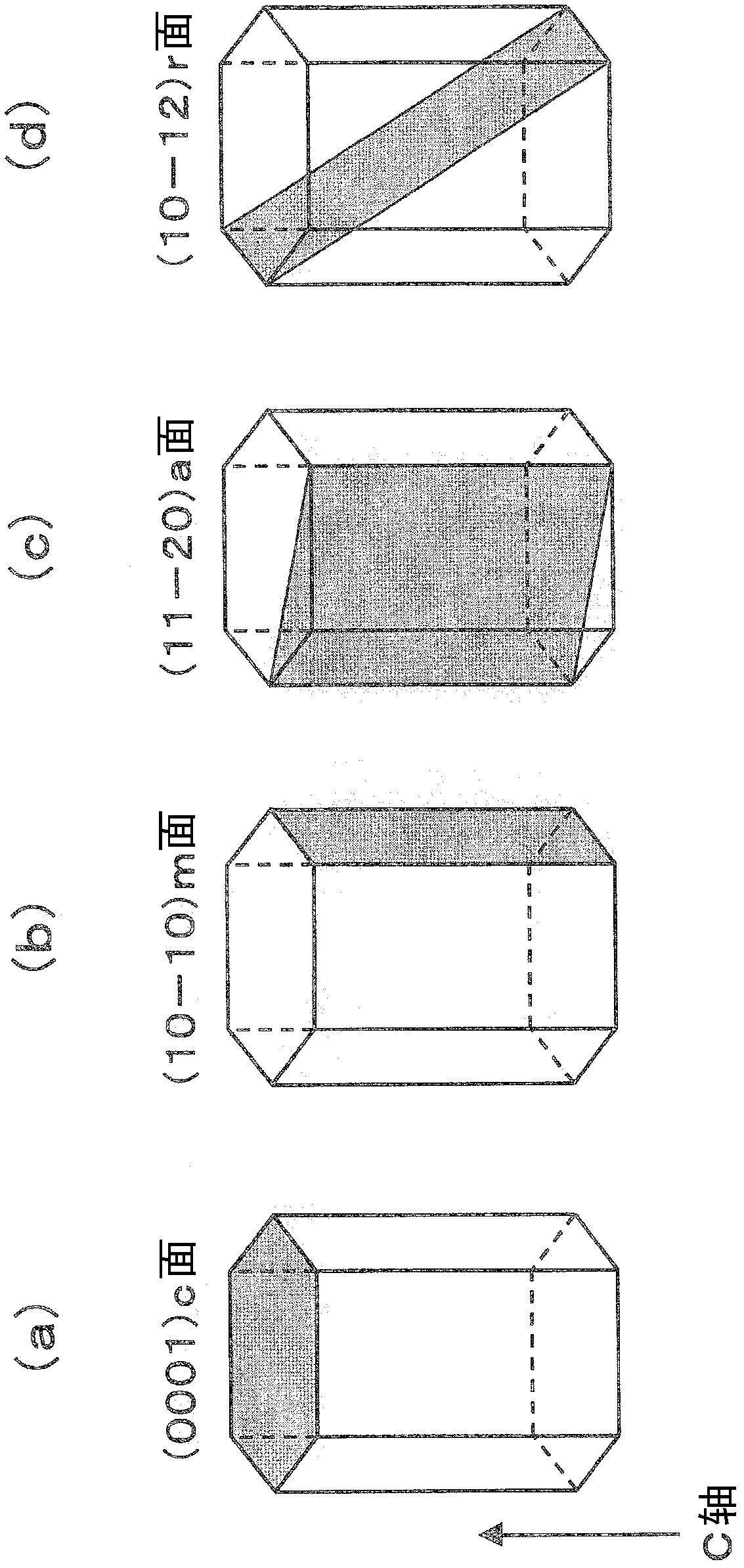
[0135] The substrate 101 for crystal growth used in this embodiment is a substrate on which gallium nitride (GaN) on the (10-10)m plane can grow. A self-supporting substrate of gallium nitride itself exhibiting an m-plane is most preferable, but a substrate exhibiting an m-plane in a 4H or 6H structure of silicon carbide (SiC) having a similar lattice constant may also be used. In addition, sapphire that also exhibits the m-plane may also be used. However, if a substance different from the gallium nitride-based compound semiconductor is used on the substrate, it is necessary to insert an appropriate intermediate layer or buffer layer between the gallium nitride-based compound semiconductor layer deposited on top.

[...


PUM


Abstract

The present invention is a method of manufacturing a gallium nitride-based compound semiconductor, including growing an m-plane InGaN layer whose emission peak wavelength is not less than 500 nm by metalorganic chemical vapor deposition. Firstly, step (A) of heating a substrate in a reactor is performed. Then, step (B) of supplying into the reactor a gas which contains an In source gas, a Ga source gas, and a N source gas and growing an m-plane InGaN layer of an InxGa1-xN crystal on the substrate at a growth temperature from 700 DEG C. to 775 DEG C. is performed. In step (B), the growth rate of the m-plane InGaN layer is set in a range from 4. 5 nm / min to 10 nm / min.

Description

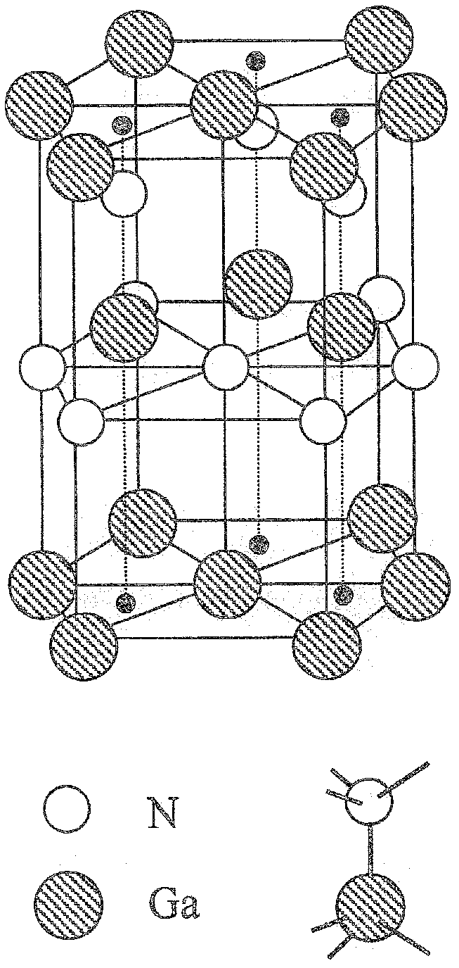
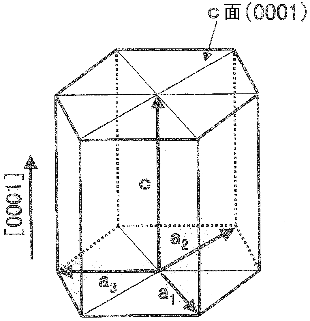
technical field [0001] The present invention relates to a method for producing a gallium nitride-based compound semiconductor, and a semiconductor light-emitting device produced by the method. Background technique [0002] Nitride semiconductors containing nitrogen (N), which is a Group V element, are promising as materials for short-wavelength light-emitting devices due to the size of their band gaps. Among them, research on gallium nitride-based compound semiconductors (GaN-based semiconductors) is flourishing, and semiconductor lasers made of blue light-emitting diodes (LEDs), green LEDs, and GaN-based semiconductors have also been put into practical use. [0003] Gallium nitride-based semiconductors have a wurtzite crystal structure. figure 1 A unit cell of GaN is schematically represented. in Al a Ga b In C In N (0≤a, b, c≤1, a+b+c=1) semiconductor crystals, figure 1 A part of Ga shown can be replaced with Al and / or In. [0004] figure 2 Indicates the four basi...

Claims


Application Information

Patent Timeline
Patent Type & Authority Applications(China)
IPC IPC(8): H01L21/205C23C16/34H01L33/06H01L33/32
CPCC23C16/303H01L33/007C30B29/403C30B25/02
Inventor 加藤亮藤金正树井上彰横川俊哉
Owner PANASONIC CORP
Learn More