Luminous device with superlattice structure active layer
A light-emitting device and superlattice technology, applied in semiconductor devices, electrical components, circuits, etc., can solve the problems of low luminous efficiency of light-emitting devices, improve crystal quality and luminous efficiency, reduce crystal defect density, improve stability and reliability effect
- Summary
- Abstract
- Description
- Claims
- Application Information
AI Technical Summary
Problems solved by technology
Method used
Image
Examples
Embodiment 1
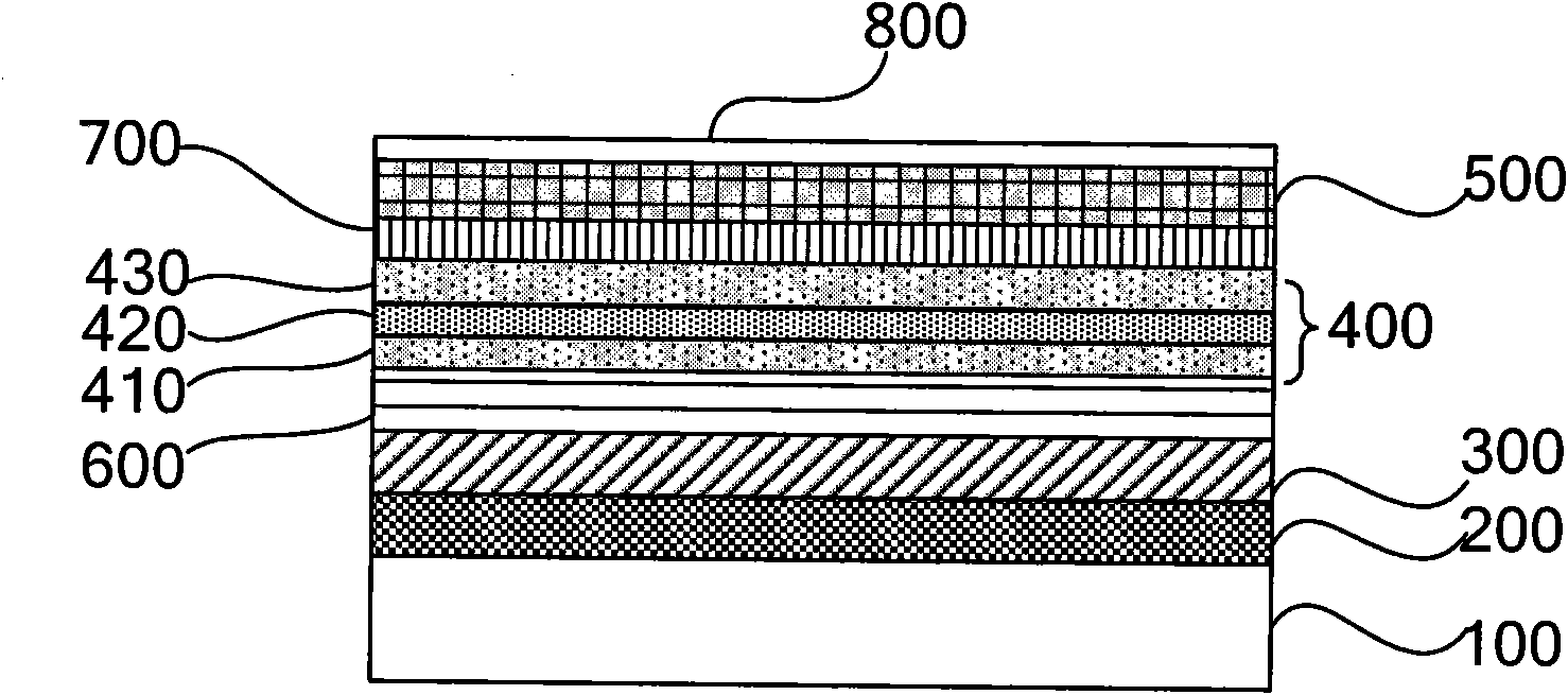
[0017] figure 2 It is a structural schematic diagram of the light-emitting device of Embodiment 1 of the present invention.
[0018] refer to figure 2 , a light emitting device according to Embodiment 1 of the present invention is proposed, and the light emitting device in this embodiment is a superlattice single quantum well light emitting device. The light-emitting device includes a sapphire substrate 100, a buffer layer 200 formed on the sapphire substrate 100 (the material of the buffer layer 200 is a gallium nitride semiconductor layer, also called a gallium nitride buffer layer 200), and a buffer layer 200 formed on the buffer layer 200. The first semiconductor layer 300 (also called N-type gallium nitride semiconductor layer 300), the first superlattice semiconductor layer 600 formed on the first semiconductor layer 300, and the organic layer formed on the first superlattice semiconductor layer 600 The source layer 400 (also called superlattice quantum well layer 40...
Embodiment 2
[0036] image 3 It is a structural schematic diagram of the light emitting device of the second embodiment of the present invention.
[0037] refer to image 3 , the light-emitting device of the second embodiment of the present invention is proposed. The light-emitting device in this embodiment is proposed on the basis of the light-emitting device in Embodiment 1, and the light-emitting device includes a sapphire substrate 100, a buffer layer 200 formed on the sapphire substrate 100, a first buffer layer 200 formed on the buffer layer 200 A semiconductor layer 300, a first superlattice semiconductor layer 600 formed on the first semiconductor layer 300, an active layer 400 formed on the first superlattice semiconductor layer 600, and a first superlattice semiconductor layer formed on the active layer 400 Two semiconductor layers 500, wherein the active layer 400 includes a first barrier layer 410, a superlattice potential well layer 420 formed on the first barrier layer 410,...
Embodiment 3
[0040] Figure 4 It is a structural schematic diagram of a light emitting device according to Embodiment 3 of the present invention.
[0041] This embodiment is proposed on the basis of the second embodiment, and the difference from the light-emitting device of the second embodiment lies in the superlattice quantum well layer. The superlattice quantum well layer in this embodiment is a superlattice multiple quantum well layer. The so-called superlattice multiple quantum well layer means that the superlattice quantum well layer has multiple superlattice potential well layers. The superlattice multiple quantum well layer 400 includes alternately stacked potential barrier layers and superlattice potential well layers. The superlattice multiple quantum well layer 400 includes multiple potential barrier layers and multiple superlattice potential well layers. In this embodiment, the barrier layer of the superlattice multi-quantum well layer 400 is preferably connected to the secon...
PUM
| Property | Measurement | Unit |
|---|---|---|
| Thickness | aaaaa | aaaaa |
| Thickness | aaaaa | aaaaa |
| Thickness | aaaaa | aaaaa |
Abstract
Description
Claims
Application Information
 - Generate Ideas
- Intellectual Property
- Life Sciences
- Materials
- Tech Scout
- Unparalleled Data Quality
- Higher Quality Content
- 60% Fewer Hallucinations
Browse by: Latest US Patents, China's latest patents, Technical Efficacy Thesaurus, Application Domain, Technology Topic, Popular Technical Reports.
© 2025 PatSnap. All rights reserved.Legal|Privacy policy|Modern Slavery Act Transparency Statement|Sitemap|About US| Contact US: help@patsnap.com


