Projection photoetching system with composite photon sieve

A lithography system and photon sieve technology, applied in microlithography exposure equipment, optics, photography, etc., can solve the problems of low efficiency and achieve the effects of high efficiency, light weight, and improved signal-to-noise ratio

Active Publication Date: 2013-03-06
INST OF MICROELECTRONICS CHINESE ACAD OF SCI
View PDF4 Cites 0 Cited by
  • Summary
  • Abstract
  • Description
  • Claims
  • Application Information

AI Technical Summary

Problems solved by technology

[0005] However, both the zone plate maskless direct writing system and the photon sieve maskless direct writing system belong to the direct writing lithography system, which cannot achieve fast mass lithography through the mask, and the efficiency is much lower than that of the projection lithography system.

Method used


Image

  • Projection photoetching system with composite photon sieve
  • Projection photoetching system with composite photon sieve
  • Projection photoetching system with composite photon sieve

Examples


Embodiment Construction

[0027] In order to make the object, technical solution and advantages of the present invention clearer, the present invention will be described in further detail below in conjunction with specific embodiments and with reference to the accompanying drawings.

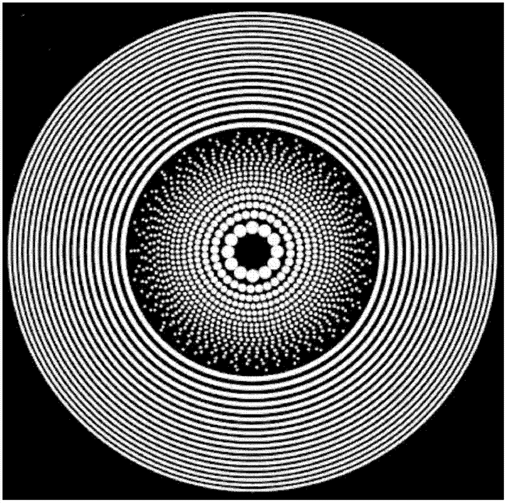
[0028] The compound photon sieve projection lithography system provided by the present invention uses a compound photon sieve to replace the projection objective lens in a traditional projection lithography system, and includes an illumination system 1 , a mask plate 2 , a compound photon sieve 3 and a substrate 4 placed in sequence. Among them, the illumination system 1 is used to generate incident light, and irradiate the incident light to the mask plate 2; the mask plate 2 is used to provide the imaging object space of the compound photon sieve 3, and the incident light passes through the mask plate 2 and is irradiated to the composite photon The sieve 3; the compound photon sieve 3 is used to realize the imaging functi...


PUM

PropertyMeasurementUnit
thicknessaaaaaaaaaa

Abstract

The invention relates to the technical field of micro-nanometer processing and discloses a projection photoetching system with a composite photon sieve. The system comprises a lighting system, a mask plate, the composite photon sieve and a substrate, which are sequentially arranged, wherein the lighting system is used for generating an incident light and emitting the incident light to the mask plate; the mask plate is used for providing an object space for imaging the composite photon sieve and emitting the incident light to the composite photon sieve through the mask plate; the composite photon sieve is used for realizing an imaging function and imaging a graph on the mask plate on the substrate; and the substrate is used for receiving an image, formed by the composite photon sieve, of the graph on the mask plate. The composite photon sieve projection photoetching system has the advantages that: because the composite photon sieve is adopted to replace a projection objective in the conventional projection photoetching system, the advantage of high efficiency of the conventional projection photoetching system can be reserved, quick massive photoetching is realized, photoetching efficiency is improved, cost can be effectively reduced, and the volume of the system is reduced.

Description

technical field [0001] The invention relates to the technical field of micro-nano processing, in particular to a composite photon sieve projection photolithography system. Background technique [0002] The projection lithography system is commonly used in the current integrated circuit manufacturing process, that is, the projection objective lens is used to reduce the image on the mask plate on the substrate surface, and then combine with other process steps to realize the transfer of the image. The core structure of the existing projection lithography system is as follows: figure 1 As shown, it consists of an illumination system 1 , a mask plate 2 , a projection objective lens 3 and a substrate 4 . The lighting system 1 is located at the top of the system and is used to generate high-quality incident light sources. The mask plate 2 is located below the illumination system 1 and is used to provide an object space for imaging by the projection objective lens. The projectio...

Claims


Application Information

Patent Timeline
Patent Type & Authority Patents(China)
IPC IPC(8): G03F7/20G03F5/18
Inventor 谢常青高南华一磊朱效立李海亮史丽娜李冬梅刘明
Owner INST OF MICROELECTRONICS CHINESE ACAD OF SCI
Why Eureka
Try Eureka