Method for manufacturing memory cell including resistor
A storage unit and manufacturing method technology, applied in the direction of electrical components, information storage, static memory, etc., to achieve the effect of high-density integration and excellent interface characteristics
- Summary
- Abstract
- Description
- Claims
- Application Information
AI Technical Summary
Problems solved by technology
Method used
Image

Examples
example
[0024] As an illustrative example, the method includes steps executed in the following order.
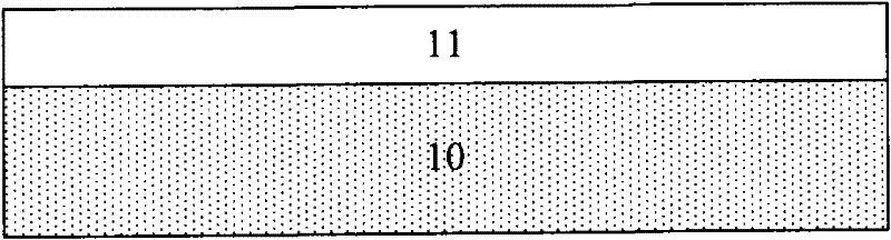
[0025] See figure 1 , Prepare insulating substrate. The insulating substrate may be a laminated substrate whose surface layer is an oxide layer.
[0026] For example, the insulating substrate includes a single crystal Si base layer (base) 10 and SiO 2 Layer 11 laminated substrate. A part of the single crystal Si underlayer 10 can be converted into SiO by thermal oxidation 2 . Or, instead, SiO is formed on the single crystal Si underlayer 10 by a chemical vapor deposition (CVD) method. 2 Layer 11.
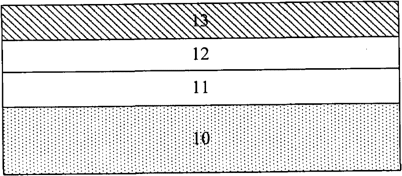
[0027] See figure 2 , By sputtering or evaporation, in SiO 2 A Ti layer 12 is formed on the layer 11 as an adhesion layer, and then a bottom electrode layer 13 (such as Pt) is formed on the Ti layer 12 by sputtering, evaporation or MOCVD.
[0028] The Ti layer 12 is an optional layer and is mainly used to improve the adhesion strength of the bottom electrode layer 13 on the substrate.
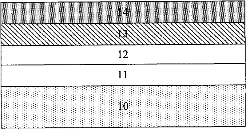
[0029]...
example 1
[0069] Example 1: Using MOCVD method to manufacture Si / SiO 2 / Ti / Pt / HfO 2 / TiN structure RRAM memory cell
[0070] Using Si crystal thermal oxidation to produce SiO 2 Insulation layer, using sputtering method in Si / SiO 2 Ti film is fabricated on top, and Si / SiO 2 The / Ti structure is placed in the MOCVD reaction chamber.
[0071] First, a Pt metal bottom electrode is manufactured. With platinum acetylacetonate as the precursor, it is sublimated at 150℃ to form platinum acetylacetonate gas, using Ar 2 As a carrier gas into the reaction chamber, O 2 As the reaction gas is introduced into the reaction chamber, the substrate temperature is maintained at 400 ℃, and the pressure of the reaction chamber is at 100 Pa. 2 Pt film is formed on Ti substrate to obtain Si / SiO 2 / Ti / Pt structure.
[0072] Use Hf(OC 2 H 5 ) 4 As the precursor, the solid alkoxide is dissolved in isopropanol to form a liquid precursor, which evaporates to form Hf(OC 2 H 5 ) 4 Gas, using Ar 2 As a carrier into the reac...
example 2
[0076] Example 2: Using MOCVD method to manufacture Si / SiO 2 / Ti / Pt / Zr 0.99 La 0.01 O 2 / Pt structure RRAM storage unit
[0077] Using Si crystal thermal oxidation to produce SiO 2 Insulation layer, using evaporation method in Si / SiO 2 Ti film is fabricated on top, and Si / SiO 2 The / Ti structure is placed in the MOCVD reaction chamber.
[0078] First, a Pt metal bottom electrode is manufactured. Platinum solid acetylacetonate is used as the precursor to sublime at 150℃ to form platinum acetylacetonate gas, using Ar 2 As a carrier gas into the reaction chamber, oxygen as a reaction gas into the reaction chamber, the substrate temperature is maintained at 500 ℃, the pressure of the reaction chamber is 100 Pa, in Si / SiO 2 Pt film is formed on the substrate to obtain Si / SiO 2 / Ti / Pt structure.
[0079] Use Zr(tmhd) 4 Solid and La(tmhd) 3 As a precursor, according to the molar ratio of Zr and La and the average speed of the deposition of the two metals, the required amount of the two prec...
PUM
 Abstract
Description
Claims
Application Information
 - R&D
- Intellectual Property
- Life Sciences
- Materials
- Tech Scout
- Unparalleled Data Quality
- Higher Quality Content
- 60% Fewer Hallucinations
Browse by: Latest US Patents, China's latest patents, Technical Efficacy Thesaurus, Application Domain, Technology Topic, Popular Technical Reports.
© 2025 PatSnap. All rights reserved.Legal|Privacy policy|Modern Slavery Act Transparency Statement|Sitemap|About US| Contact US: help@patsnap.com