Integrated circuit element, forming method thereof and packaging assembly
A technology for integrated circuits and packaging components, which is applied in the field of bump structures, and can solve the problems of solder wetting to the side walls, high manufacturing cost interface delamination, etc.
- Summary
- Abstract
- Description
- Claims
- Application Information
AI Technical Summary
Problems solved by technology
Method used
Image
Examples
Embodiment Construction
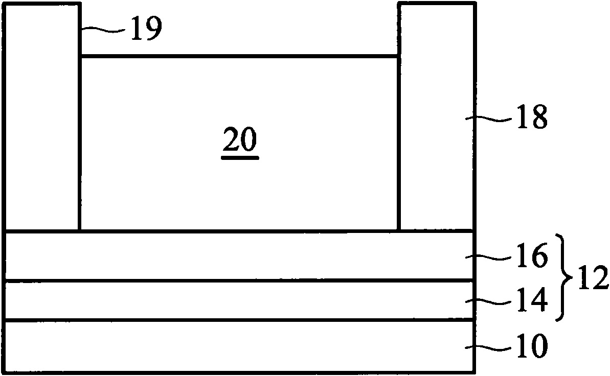
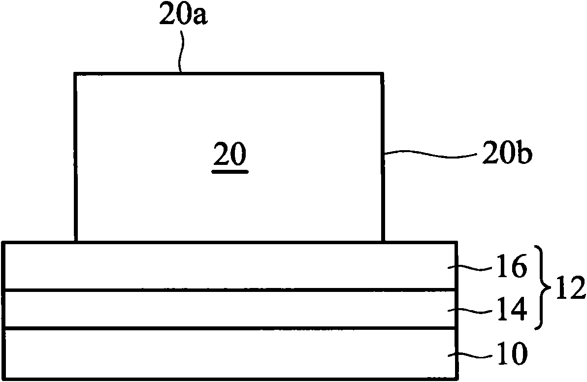
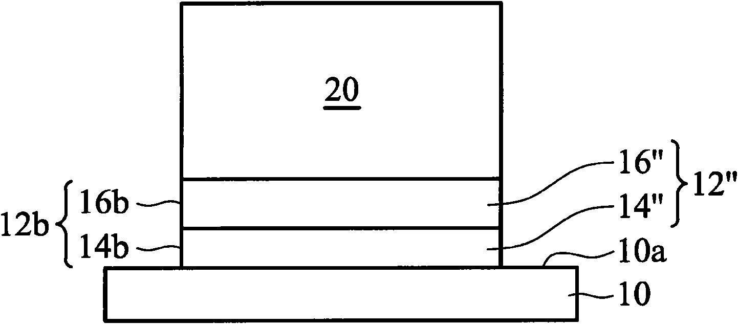
[0033] Embodiments disclosed herein provide a sidewall protection process for copper pillar bump technology, wherein the L-shaped protection structure on the sidewall of the copper pillar bump is formed of at least one layer of non-metallic material, such as a dielectric material layer, polymer material layer or a combination of the foregoing. The term "copper pillar bump" used throughout this disclosure refers to bump structures, including conductive pillars formed of copper or copper alloys, which can be directly applied to flip-chip assemblies or other similar applications On the electrical pad or on the redistribution layer of the semiconductor chip.
[0034] In the embodiments of the present invention, reference materials are used to describe the present invention in detail. As shown in the drawings, the same reference numerals are used as much as possible in the drawings and descriptions to indicate the same or similar parts. In the drawings, the shapes and thicknesses ...
PUM
 Abstract
Description
Claims
Application Information
 - Generate Ideas
- Intellectual Property
- Life Sciences
- Materials
- Tech Scout
- Unparalleled Data Quality
- Higher Quality Content
- 60% Fewer Hallucinations
Browse by: Latest US Patents, China's latest patents, Technical Efficacy Thesaurus, Application Domain, Technology Topic, Popular Technical Reports.
© 2025 PatSnap. All rights reserved.Legal|Privacy policy|Modern Slavery Act Transparency Statement|Sitemap|About US| Contact US: help@patsnap.com


