Method for manufacturing GaN (gallium nitride) substrate
A substrate and transition layer technology, applied in the field of GaN substrate preparation, can solve the problems of low yield, high price, complicated process, etc.
- Summary
- Abstract
- Description
- Claims
- Application Information
AI Technical Summary
Problems solved by technology
Method used
Image
Examples
Embodiment 1
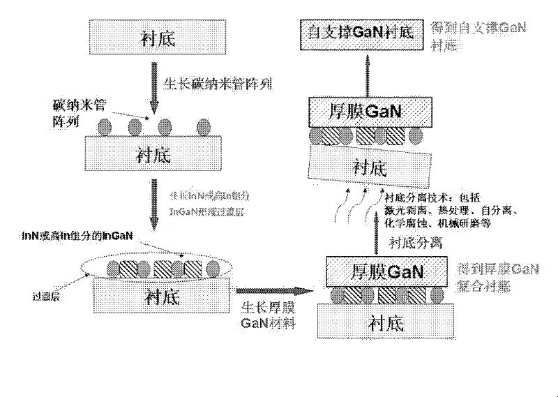
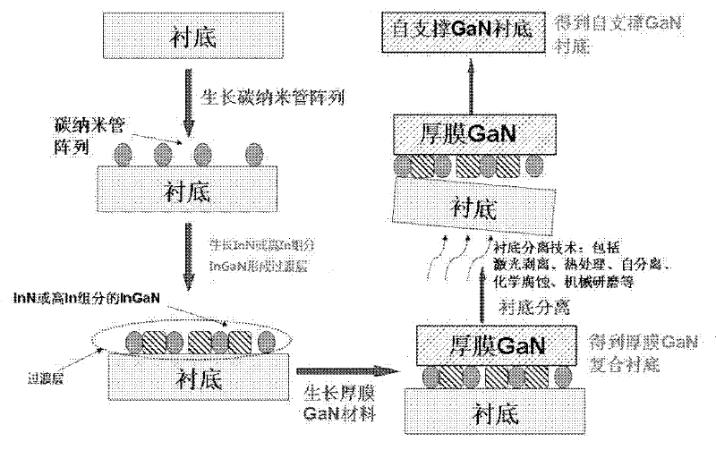
[0025] Embodiment 1: Preparation of c-plane self-supporting GaN substrate, as shown in the accompanying drawings:
[0026] 1) The substrate can be sapphire, silicon carbide, Si and other substrates, or GaN, AlN, InN or other III-nitride material thin films grown on sapphire, silicon carbide, Si and other substrates. Arrange carbon nanotubes in parallel on the substrate, the arrangement is parallel arrangement along the growth plane, the arrangement can be isoperiodic, or a periodic disordered structure, the carbon nanotubes can be a single carbon nanotube or a group of carbon nanotubes Clusters of carbon nanotubes, in various forms such as single-layer or multi-layer. The present embodiment selects the sapphire substrate of c plane, selects the single-layer carbon nanotubes arranged vertically along the reference side of the substrate at equal periods; the diameter of the carbon nanotubes is 1-100 nanometers, and this embodiment adopts 5 nanometers; the period is 1 -100 micro...
Embodiment 2
[0033] Embodiment 2: Preparation of c-plane GaN thick film substrate:
[0034] 1) The substrate is sapphire, silicon carbide, Si and other substrates, or GaN, AlN, InN or other III-nitride material films grown on sapphire, silicon carbide, Si and other substrates; Single-layer carbon nanotubes arranged in the vertical direction of the bottom reference side; the diameter of the carbon nanotubes is 1-100 nanometers, which is 5 nanometers in this embodiment; the period is 1-100 microns, preferably 1-10 microns, and 2 microns is used in this embodiment ;
[0035] 2) Use MBE growth technology to grow In 0.9 Ga 0.1 N material, composed of carbon nanotubes and In 0.9 Ga 0.1 N transition layer. In 0.9 Ga 0.1 The thickness of the N material is 10 nanometers to 500 nanometers, and 100 nanometers is used in this embodiment. The MBE growth temperature is 400-450 degrees, and 420 degrees is used in this embodiment.
[0036] 3) GaN material is grown using MOCVD growth technology. ...
Embodiment 3
[0040] Embodiment 3: Preparation of non-polar a-plane self-supporting GaN or thick film composite substrate:
[0041] 1) The substrate is r-plane sapphire, silicon carbide, Si and other substrates, or GaN, AlN, InN or other group III nitride material films grown on sapphire, silicon carbide, Si and other substrates; carbon nanotubes The arrangement is a parallel arrangement along the growth plane, and the arrangement can be isoperiodic or periodic disordered structure. The carbon nanotubes can be a single carbon nanotube, or a cluster of carbon nanotubes and other forms: this The embodiment selects the r-face sapphire substrate, and selects single-layer carbon nanotubes arranged along the vertical direction of the substrate reference edge with equal periods; the diameter of the carbon nanotubes is 1-100 nanometers, and this embodiment adopts 5 nanometers; the period is 1-100 nanometers. Micron, preferably 1-10 micron, the present embodiment adopts 2 micron;
[0042] 2) Using ...
PUM
| Property | Measurement | Unit |
|---|---|---|
| Thickness | aaaaa | aaaaa |
| Thickness | aaaaa | aaaaa |
| Thickness | aaaaa | aaaaa |
Abstract
Description
Claims
Application Information
 - R&D
- Intellectual Property
- Life Sciences
- Materials
- Tech Scout
- Unparalleled Data Quality
- Higher Quality Content
- 60% Fewer Hallucinations
Browse by: Latest US Patents, China's latest patents, Technical Efficacy Thesaurus, Application Domain, Technology Topic, Popular Technical Reports.
© 2025 PatSnap. All rights reserved.Legal|Privacy policy|Modern Slavery Act Transparency Statement|Sitemap|About US| Contact US: help@patsnap.com


