Preparation method for photoanode of dye-sensitized solar cell
A solar cell and dye sensitization technology, which is applied in the field of preparing dye-sensitized solar cells (DSSC) photoanodes, can solve the problems of disordered semiconductor crystal plane orientation and easy peeling off of semiconductor thin films, and achieve film formation conditions and easy thickness The effect of control, low preparation cost and high flatness
- Summary
- Abstract
- Description
- Claims
- Application Information
AI Technical Summary
Problems solved by technology
Method used
Image


Examples
Embodiment 1
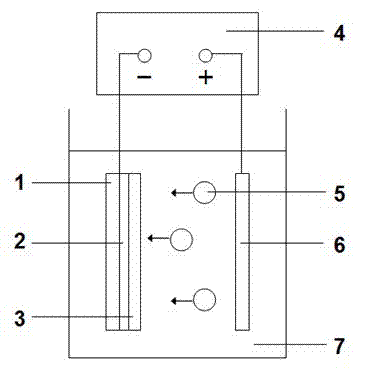
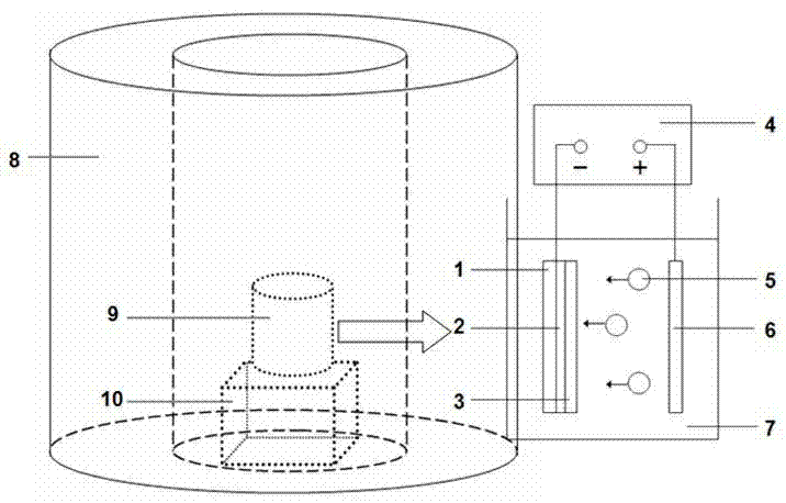
[0026] SnO doped with fluorine 2 Conductive glass (SnO 2 : F, referred to as FTO) is the photoanode electrode base material, the base thickness is 2.2 mm, the visible light transmittance is 90%, and the surface sheet resistance is 14 Ω / □;
[0027] A layer of dense TiO with a thickness of about 50 nm was sputtered on the surface of FTO conductive glass by magnetron sputtering 2 layer as a barrier layer.
[0028] Mix isopropanol solution with TiO 2 After the particles are mixed, they are ultrasonically dispersed to make an electrophoretic fluid.
[0029] In a strong magnetic field, dense TiO is deposited by electrophoresis 2 barrier layer on the FTO conductive substrate.
[0030] The film prepared above was sintered in a muffle furnace at 450° C. for 30 minutes to increase the crystallinity of semiconductor nanoparticles.
[0031] Adsorbs dyes. The above electrode was heated at 80 °C for 20 minutes and then immersed in an ethanol solution of N3 dye (purchased...
Embodiment 2
[0037] The FTO conductive glass is used as the substrate material of the photoanode electrode, the thickness of the substrate is 2.2 mm, the visible light transmittance is 90%, and the surface sheet resistance is 14 Ω / □.
[0038] A layer of dense TiO with a thickness of about 200 nm was sputtered on the surface of FTO conductive glass by magnetron sputtering 2 layer as a barrier layer.
[0039] Mix isopropanol solution with TiO 2 After the particles are mixed, they are ultrasonically dispersed to make an electrophoretic fluid.
[0040] In a strong magnetic field, dense TiO is deposited by electrophoresis 2 barrier layer on the FTO conductive substrate.
[0041] The film prepared above was sintered in a muffle furnace at 450° C. for 30 minutes to increase the crystallinity of semiconductor nanoparticles.
[0042] Adsorbs dyes. The above electrode was heated at 80 °C for 20 minutes and then immersed in an ethanol solution of N719 dye (purchased by DYESOL, Austr...
Embodiment 3
[0048] The FTO conductive glass is used as the substrate material of the photoanode electrode, the thickness of the substrate is 2.2 mm, the visible light transmittance is 90%, and the surface sheet resistance is 14 Ω / □.
[0049] A layer of dense TiO with a thickness of about 300 nm was sputtered on the surface of FTO conductive glass by magnetron sputtering 2 layer as a barrier layer.
[0050] ethanol solution with TiO 2 After the particles are mixed, they are ultrasonically dispersed to make an electrophoretic fluid.
[0051] In a strong magnetic field, dense TiO is deposited by electrophoresis 2 barrier layer on the FTO conductive substrate.
[0052] The film prepared above was sintered in a muffle furnace at 450° C. for 30 minutes to increase the crystallinity of semiconductor nanoparticles.
[0053] Adsorbs dyes. The above electrode was heated at 80 °C for 20 minutes and then immersed in an ethanol solution of N3 dye (purchased by DYESOL, Australia) (the...
PUM
| Property | Measurement | Unit |
|---|---|---|
| thickness | aaaaa | aaaaa |
| concentration | aaaaa | aaaaa |
| concentration | aaaaa | aaaaa |
Abstract
Description
Claims
Application Information
 - Generate Ideas
- Intellectual Property
- Life Sciences
- Materials
- Tech Scout
- Unparalleled Data Quality
- Higher Quality Content
- 60% Fewer Hallucinations
Browse by: Latest US Patents, China's latest patents, Technical Efficacy Thesaurus, Application Domain, Technology Topic, Popular Technical Reports.
© 2025 PatSnap. All rights reserved.Legal|Privacy policy|Modern Slavery Act Transparency Statement|Sitemap|About US| Contact US: help@patsnap.com