Method for manufacturing terminal structure of deep-groove super-junction metal oxide semiconductor (MOS) device

A technology of MOS device and terminal structure, applied in semiconductor/solid-state device manufacturing, semiconductor devices, electrical components, etc., can solve problems such as very high process consistency requirements and complex structure design, achieve obvious voltage division effect and reduce surface electric field. , the effect of saving terminal area

Inactive Publication Date: 2011-10-12
ADVANCED SEMICON MFG CO LTD
View PDF7 Cites 3 Cited by
  • Summary
  • Abstract
  • Description
  • Claims
  • Application Information

AI Technical Summary

Problems solved by technology

If only a simple guard ring structure is used, not only the structural design is complicated, but also the requirements for the consistency of the process are very high

Method used


Image

  • Method for manufacturing terminal structure of deep-groove super-junction metal oxide semiconductor (MOS) device
  • Method for manufacturing terminal structure of deep-groove super-junction metal oxide semiconductor (MOS) device
  • Method for manufacturing terminal structure of deep-groove super-junction metal oxide semiconductor (MOS) device

Examples


Embodiment Construction

[0039] The present invention will be further described below in conjunction with specific embodiments and accompanying drawings, but the protection scope of the present invention should not be limited thereby.

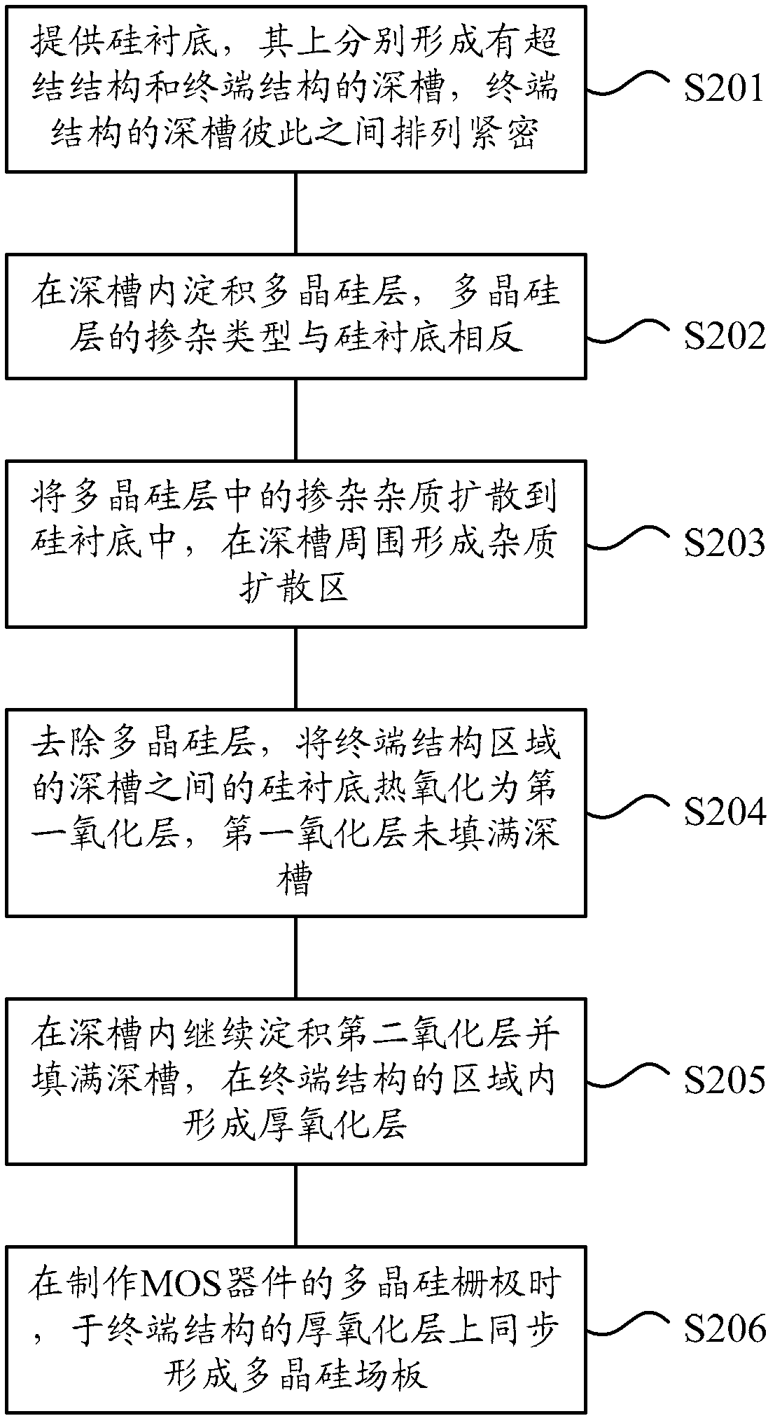
[0040] figure 1 It is a schematic flow chart of a manufacturing method for a terminal structure of a deep-trench super-junction MOS device according to an embodiment of the present invention. As shown in the figure, the manufacturing method of the terminal structure may include:

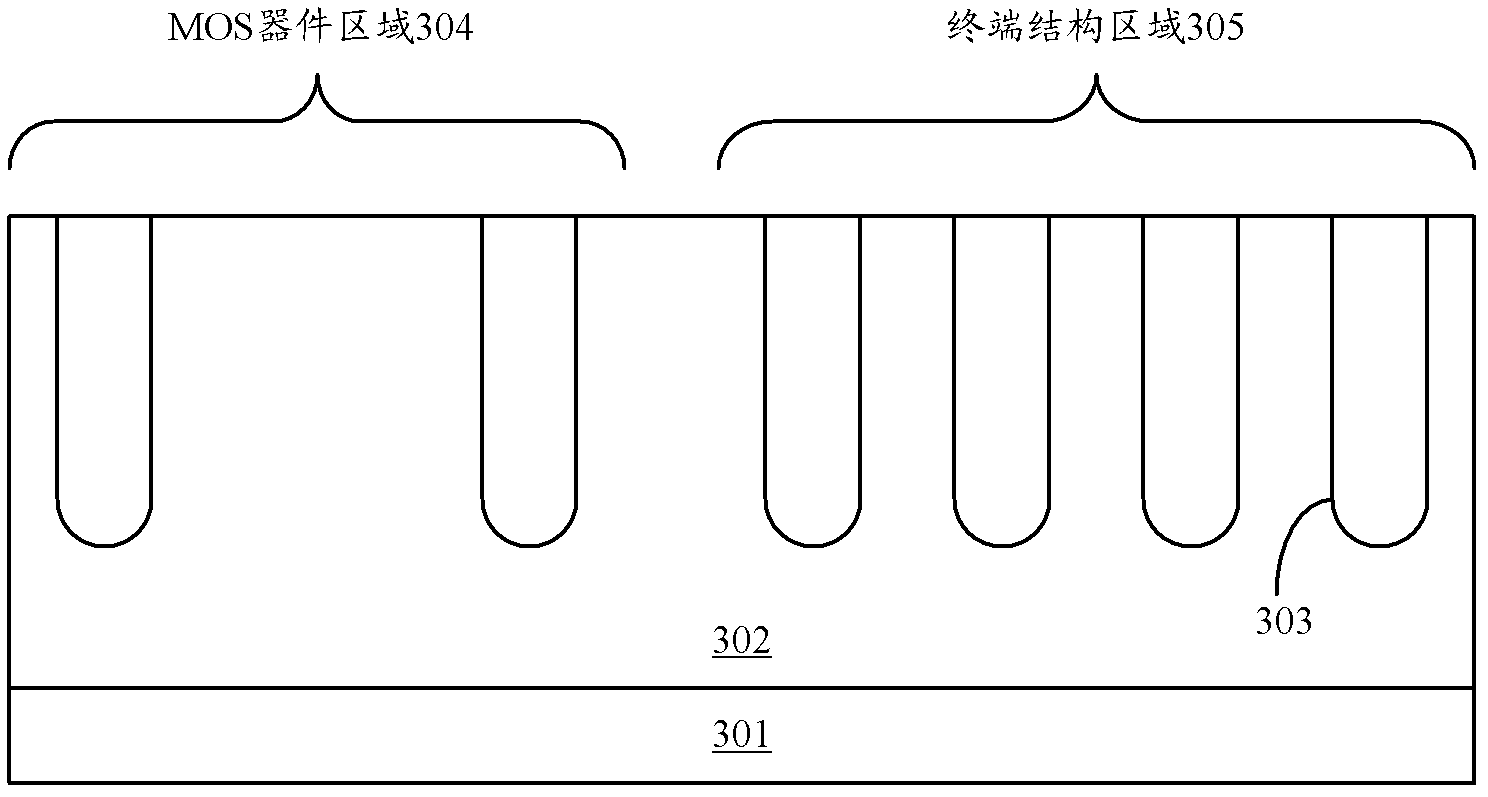
[0041] Step S101 is performed to provide a silicon substrate on which deep grooves of a super junction structure and a terminal structure are respectively formed, and the deep grooves of the terminal structure are closely arranged with each other;

[0042] Execute step S102, depositing a polysilicon layer in the deep groove, the doping type of the polysilicon layer is opposite to that of the silicon substrate;

[0043] Executing step S103, diffusing dopant impurities in the polysilicon laye...


PUM

PropertyMeasurementUnit
thicknessaaaaaaaaaa
thicknessaaaaaaaaaa

Abstract

The invention provides a method for manufacturing a terminal structure of a deep-groove super-junction metal oxide semiconductor (MOS) device, which comprises the following steps of: providing a silicon substrate, wherein deep grooves with a super-junction structure and a terminal structure are formed on the silicon substrate respectively, and the deep grooves with the terminal structure are formed closely; depositing polycrystalline silicon layers in the deep grooves, wherein the doping type of the polycrystalline silicon layers is opposite to that of the silicon substrate; diffusing doped impurities in the polycrystalline silicon layers to the silicon substrate, and forming impurity diffusion areas at the peripheries of the deep grooves; performing thermal oxidation on the silicon substrate between the polycrystalline silicon layers and the deep grooves in a terminal structure area to form oxide layers for completely filling the deep grooves, and forming a thick oxide layer in the terminal structure area; and synchronously forming a polycrystalline silicon field plate on the thick oxide layer in the terminal structure area when a polycrystalline silicon grid of the MOS device is manufactured. The field plate is formed by the polycrystalline silicon grid in the terminal structure area and is combined with the thick oxide layer, and the voltage division effect of the thick oxide layer is effectively utilized, so that the surface field of the device is reduced; and by combining the effects of a deep groove reduced surface field (RESURF) and the field plate, the pressure division effect is obvious, and the area of a terminal is reduced to a great extent.

Description

technical field [0001] The invention relates to the technical field of semiconductor manufacturing, in particular, the invention relates to a manufacturing method for a terminal structure of a deep groove super junction MOS device. Background technique [0002] Power MOSFET is widely used in medium and low voltage due to its high input impedance, low loss, fast switching speed, no secondary breakdown, wide safe working area, good dynamic performance, easy coupling with the front pole to achieve large current, and high conversion efficiency. power conversion and control field. Although power MOS devices have been amazingly improved in terms of power handling capability, in the high-voltage field due to the on-resistance Ron, the conduction loss of power MOS devices increases rapidly with the increase of withstand voltage. In order to improve withstand voltage and reduce conduction loss, a series of new structures and technologies have emerged. Among them, the super junction...

Claims


Application Information

Patent Timeline
Patent Type & Authority Applications(China)
IPC IPC(8): H01L21/336H01L21/28
Inventor 永福龚大卫陈雪萌陆昉缪润妍
Owner ADVANCED SEMICON MFG CO LTD
Why Eureka
Try Eureka