Method for manufacturing back contact HIT (Heterojunction with Intrinsic Thin Layer) solar cell based on P-type silicon chip
A solar cell and back-contact technology, which is applied in the manufacture of circuits, electrical components, and final products, can solve the problems of small production capacity and high cost, and achieve the effects of simple method, reduced component production cost, and long optical path
- Summary
- Abstract
- Description
- Claims
- Application Information
AI Technical Summary
Problems solved by technology
Method used
Image
Examples
Embodiment 1
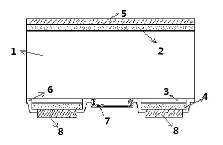
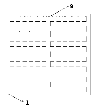
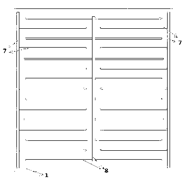
[0031] Select P-type monocrystalline silicon wafer; P-type silicon wafer 1 undergoes a conventional cleaning process, and the surface is subjected to alkali texturing to remove the mechanical damage layer on the surface of the silicon wafer, remove surface oil and metal impurities, and form a pyramid-shaped textured surface. Increase the absorption of sunlight, increase the area of the PN junction, and increase the short-circuit current. A layer of highly doped P+-type amorphous silicon thin layer 2 is deposited on the front surface of P-type silicon wafer 1 by amorphous silicon coating equipment, the film thickness is 50nm, and then a layer of intrinsic amorphous silicon is sequentially deposited on the back surface The thin silicon layer 3 has a film thickness of 1 nm, and the thin N-type amorphous silicon layer 4 has a film thickness of 150 nm. On the screen printing machine, according to the drawings in the manual figure 2 As shown in the mask pattern, SiO is printed o...
Embodiment 2
[0033] Select P-type polysilicon wafers; P-type silicon wafers 1 undergo a conventional cleaning process, and carry out alkali texturing on the surface, so as to remove the mechanical damage layer on the surface of the silicon wafer, remove surface oil and metal impurities, and form a pyramid-shaped textured surface to increase The absorption of sunlight increases the area of the PN junction and increases the short-circuit current. A layer of highly doped P+-type amorphous silicon thin layer 2 is deposited on the front surface of P-type silicon wafer 1 by amorphous silicon coating equipment, the film thickness is 50nm, and then a layer of intrinsic amorphous silicon is sequentially deposited on the back surface The thin silicon layer 3 has a film thickness of 1 nm, and the thin N-type amorphous silicon layer 4 has a film thickness of 150 nm. On the screen printing machine, according to the drawings in the manual figure 2 As shown in the mask pattern, SiO is printed on the ...
PUM
| Property | Measurement | Unit |
|---|---|---|
| thickness | aaaaa | aaaaa |
| thickness | aaaaa | aaaaa |
| refractive index | aaaaa | aaaaa |
Abstract
Description
Claims
Application Information
 - R&D
- Intellectual Property
- Life Sciences
- Materials
- Tech Scout
- Unparalleled Data Quality
- Higher Quality Content
- 60% Fewer Hallucinations
Browse by: Latest US Patents, China's latest patents, Technical Efficacy Thesaurus, Application Domain, Technology Topic, Popular Technical Reports.
© 2025 PatSnap. All rights reserved.Legal|Privacy policy|Modern Slavery Act Transparency Statement|Sitemap|About US| Contact US: help@patsnap.com


