Method for synthesizing Si/IIB-VIB group semiconductor nano p-n junction with one-step method
A semiconductor and nanotechnology, applied in semiconductor/solid-state device manufacturing, gaseous chemical plating, coating, etc., can solve the problems of complex process, poor controllability, low repeatability, etc., and achieve the effect of simple process
- Summary
- Abstract
- Description
- Claims
- Application Information
AI Technical Summary
Problems solved by technology
Method used
Image

Examples
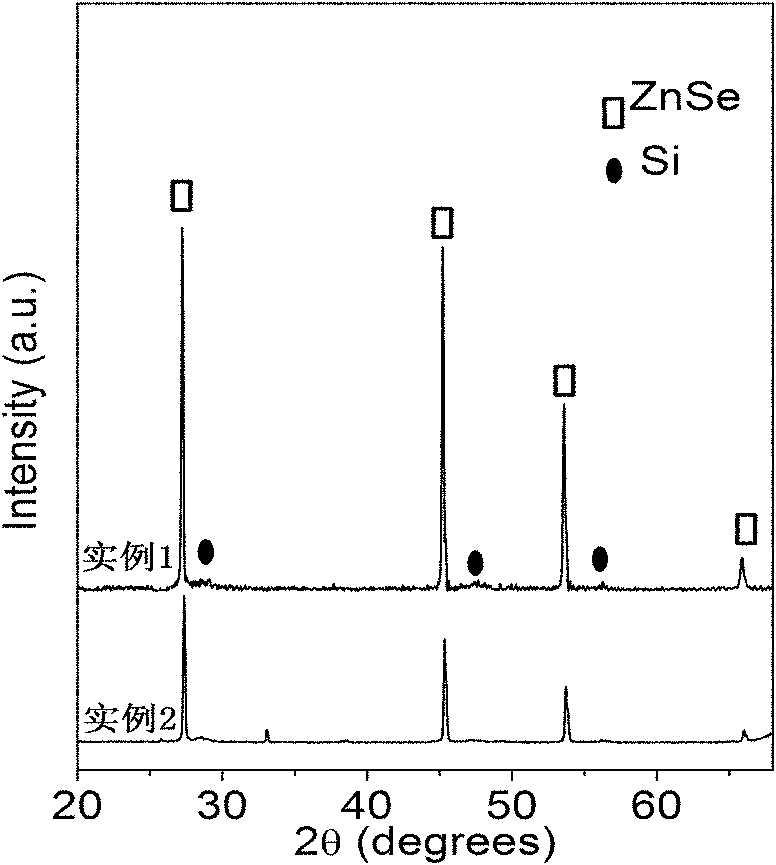
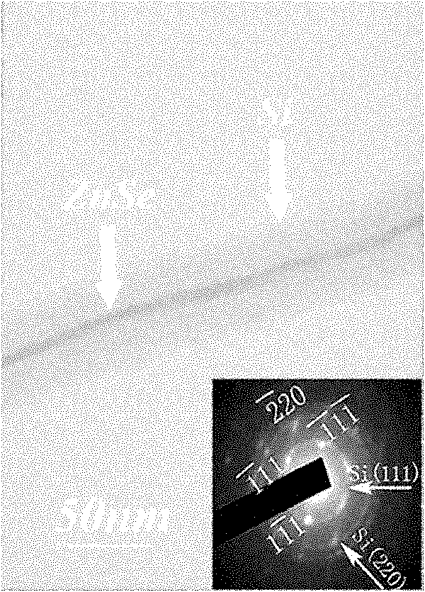
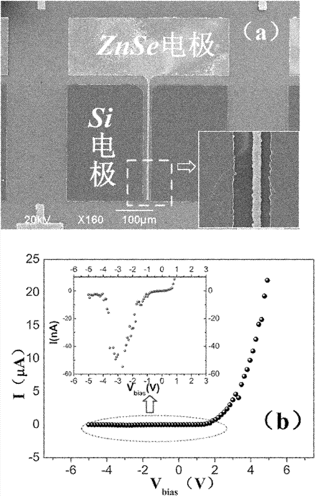
Embodiment 1
[0030] 1. Mix high-purity Sb powder (99.99%) with IIB-VIB group semiconductor ZnSe powder (99.99%) according to an atomic ratio of 8%, and put them into an agate bowl for full grinding.
[0031]2. Weigh 0.5g of mixed ZnSe and Sb powder into a small porcelain boat, and put the small porcelain boat into the center of the horizontal tube furnace. Place a vaporized gold silicon wafer 12cm away from the small porcelain boat downstream of the carrier gas. The thickness of the gold film on the evaporated gold silicon wafer is about 10nm.
[0032] 3. Use a mechanical pump and a molecular pump to pump the background vacuum in the horizontal tube furnace to 10 -3 Pa, feed high-purity argon and hydrogen, and keep the pressure in the furnace at 1.6×10 4 Pa, the flow rate of argon and hydrogen is maintained at 150SCCM.
[0033] 4. After 40 minutes, the temperature of the furnace was programmed to rise to 580°C, and high-purity silane was introduced, and the flow rate of argon-hydrogen g...
Embodiment 2
[0036] High-purity Ga powder (99.99%) is ground and mixed with IIB-VIB group semiconductor CdSe powder (99.99%) in an agate bowl at an atomic ratio of 6%, and the subsequent operations are the same as in Example 1. A Si / CdSe group semiconductor nanometer p-n junction is obtained.
Embodiment 3
[0038] 1. Weigh 1g IIB-VIB semiconductor ZnSe powder into a small porcelain boat, and put the small porcelain boat into the center of the horizontal tube furnace. Place a vaporized gold silicon wafer 12cm away from the small porcelain boat downstream of the carrier gas. The thickness of the gold film on the evaporated gold silicon wafer is about 10nm.
[0039] 2. Use a mechanical pump and a molecular pump to pump the background vacuum in the horizontal tube furnace to 10 -3 Pa, feed high-purity argon-hydrogen gas, and keep the pressure in the furnace at 6×10 3 Pa, the flow rate of argon and hydrogen is maintained at 150SCCM.
[0040] 3. After 40 minutes, the temperature of the furnace was programmed to rise to 600° C., and high-purity silane and phosphine (hydrogen diluted to 10%) were fed in. The silane flow rate was maintained at 50 SCCM, and the phosphine flow rate was 50 SCCM. The air pressure remains constant. After 30 minutes, the temperature continued to rise to 104...
PUM
| Property | Measurement | Unit |
|---|---|---|
| thickness | aaaaa | aaaaa |
| thickness | aaaaa | aaaaa |
| thickness | aaaaa | aaaaa |
Abstract
Description
Claims
Application Information
 - R&D
- Intellectual Property
- Life Sciences
- Materials
- Tech Scout
- Unparalleled Data Quality
- Higher Quality Content
- 60% Fewer Hallucinations
Browse by: Latest US Patents, China's latest patents, Technical Efficacy Thesaurus, Application Domain, Technology Topic, Popular Technical Reports.
© 2025 PatSnap. All rights reserved.Legal|Privacy policy|Modern Slavery Act Transparency Statement|Sitemap|About US| Contact US: help@patsnap.com