Charge testing method in plasma environment and testing system

A test system and plasma technology, applied in the direction of measuring devices, measuring electrical variables, instruments, etc., can solve problems such as non-reusable, unable to fully meet test requirements, plasma damage, etc.

Inactive Publication Date: 2013-05-29
PEKING UNIV
View PDF9 Cites 0 Cited by
  • Summary
  • Abstract
  • Description
  • Claims
  • Application Information

AI Technical Summary

Problems solved by technology

Plasma processing has many advantages, but as device dimensions shrink, a growing problem arises: plasma-induced damage
Such methods are destructive and cannot be reused
[0006] To sum up, we not only want to understand the distribution of charges in the plasma, but also want to get the accumulation of charges on each pixel. The existing technology cannot fully meet the testing requirements.

Method used


Image

  • Charge testing method in plasma environment and testing system
  • Charge testing method in plasma environment and testing system
  • Charge testing method in plasma environment and testing system

Examples


Embodiment Construction

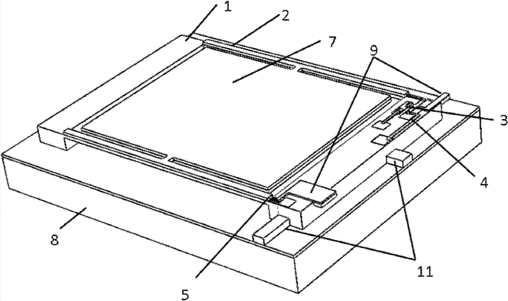
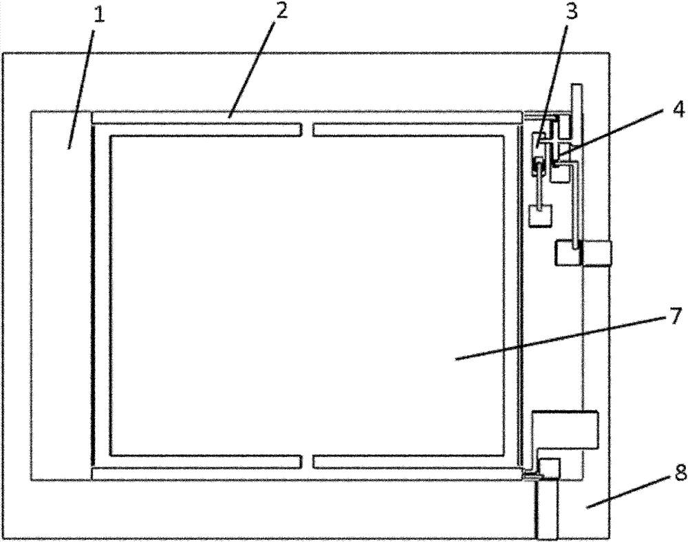
[0102] A charge detection chip that can be used to monitor plasma processing technology is prepared by monolithic integration of microelectromechanical system (MEMS) technology and IC (CMOS) technology. Such as figure 2 As shown in Figure 3, the test unit of the chip is located on the substrate 8, and consists of five main functional components: the lower plate 6, the bi-material beam 2, the piezoresistor 5, the MOS switch 4, and the protection diode 3, among which:

[0103] The double-material beam 2 is composed of a structural layer on the lower layer and a metal layer on the upper layer, and the shapes of the structural layer and the metal layer are completely coincident. The top view of the bimaterial beam 2 is a centrosymmetric figure, such as Figure 4 shown. In order to accumulate enough charges on a limited chip area, the middle of the bimaterial beam 2 is designed as a large-area rectangular flat plate, and its upper layer is the metal pole plate 7 . The central s...


PUM


Abstract

The invention discloses a charge testing method in a plasma environment and a testing system. The testing system comprises a chip integrated with MEMS (Micro-electromechanical Systems) and CMOS, and a testing circuit, wherein the chip includes a testing unit consisting of a bi-material cantilever beam temperature-sensitive structure and a structure capable of acquiring plasma density based on electrostatic suction principle; a strain resistor is used as the testing means for acquiring the deformation of the temperature-sensitive structure and a charge collection structure; and the testing circuit is used for measuring the change of the strain resistor. During charge testing, the accumulated charges are tested preliminarily; then, the released charges are re-measured to obviate the influence of an interference factor while only keeping the change influence; and the charge accumulation amount can be calculated. The system can real-time monitor the accumulation amount and the distribution of charges in the time and space domains by using a plurality of testing units arranged in an array manner, thereby providing the possibility for real-time online measurement of the plasma influenceon devices.

Description

technical field [0001] The invention belongs to the field of micro-electro-mechanical systems (MEMS) and integrated circuit IC (CMOS) processing technology, and relates to real-time monitoring of plasma technology, in particular to a method for real-time monitoring of the charge state in the plasma technology process, and related Chips and test systems integrated with MEMS and CMOS are especially used to monitor charge and uniformity in processes containing low-temperature plasma. Background technique [0002] Plasma is a form of matter under high temperature or specific excitation. It is the fourth state of matter besides solid, liquid and gas. Plasma is composed of a collection of ions, electrons, and unionized neutral particles, and is in a neutral state of matter as a whole. Plasma can be divided into high temperature and low temperature plasma. Low temperature plasma is widely used in the field of microelectronic processing. With the development of integrated circuit...

Claims


Application Information

Patent Timeline
Patent Type & Authority Patents(China)
IPC IPC(8): G01R29/24B81C99/00
Inventor 赵丹淇张大成罗葵王玮田大宇杨芳刘鹏李婷
Owner PEKING UNIV
Why Eureka
Try Eureka